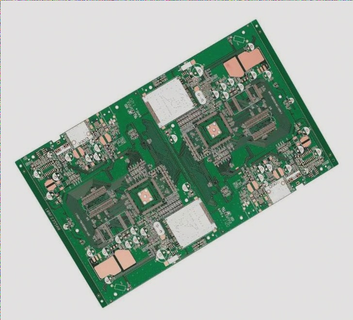
1. PCB manufacturing and PCB design have undergone significant changes in recent years. The initial board designs were rudimentary, but advancements in technology have introduced new performance criteria to the printed circuit realm, leading to increased complexity in design and manufacturing practices. Controlled impedance, a crucial approach in PCB manufacturing, addresses various factors ranging from circuit routing power to signal speed.
2. **What is impedance and its significance?**
Impedance, expressed in ohms, denotes the degree of opposition to energy flow in a circuit or transmission line. It encompasses the sum of circuit resistance and reactance, the latter resulting from two effects:
– **Inductance**: Voltage induction in a conductor due to the current’s magnetic field.
– **Capacitance**: Accumulation of static charge owing to voltage between conductors.
At low frequencies (DC), reactance is negligible, and impedance is primarily dictated by resistance. However, for high-frequency circuits, reactance and impedance become pivotal factors.
3. **Understanding Controlled Impedance**
Impedance disparities within a system can lead to failures and performance degradation. Ensuring impedance mismatches remain within acceptable bounds is a design imperative often referred to as controlled impedance. A quintessential example is coaxial cable design, featuring an inner conductor separated from the shield (outer cylindrical conductor) by an insulator. Rigorous control over insulator properties and component proportions is exercised to regulate cable impedance.
4. **The Role of LDI in PCB Manufacturing**
In PCB fabrication, traces symbolize conductors, laminates represent insulators, and planes denote shields. Consequently, a printed circuit board’s impedance hinges on the dimensions and materials utilized in the manufacturing process.
5. **Significance of Impedance Control**
Within a printed circuit board, the objective of tracing is to efficiently convey signal power from source to load. However, optimal signal transmission can only be realized if the source impedance matches the load impedance; otherwise, signal energy is reflected back to the source, compromising quality. With the proliferation of high-speed signal technologies, PCB designs incorporating controllable impedance have gained prominence.
6. **Implementing Impedance Control in PCB Production**
Impedance control in PCB fabrication and design is achieved through two primary methods: meticulous PCB stacking and trace design. It is well-established that impedance correlates with laminate height and inversely with wire width and thickness. Thus, modifying the size and spacing of specific traces enables adjustment of their impedance values.
7. **Considering Permittivity**
Finally, impedance is influenced by the layer’s permittivity—a metric quantifying a material’s inherent capacity to store electrical energy within an electric field.