In many cases, you’ll need to work across multiple programs to ensure that all aspects of your PCB design integrate seamlessly. In this guide, I’ll walk you through the process of importing DXF files into KiCad for your PCB design and how to export your PCB to be rendered in SolidWorks or other CAD software.
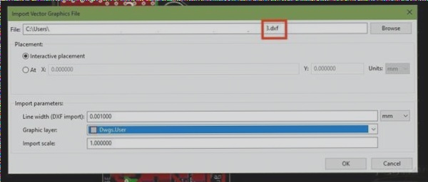
To import a DXF file into KiCad, navigate to File → Import → DXF. Ensure the file extension is .dxf (lowercase) and not .DXF (uppercase), as the import might fail depending on your KiCad version. Next, choose the appropriate layer where the file should be imported. Typically, you’ll want to import it into the Drawings layer, especially if you’re importing an outline to define the physical boundaries where the PCB will fit. Alternatively, if the DXF file represents the PCB outline along with mounting hole locations, you may opt for the Edge.Cuts layer. However, this is less common in most design scenarios.
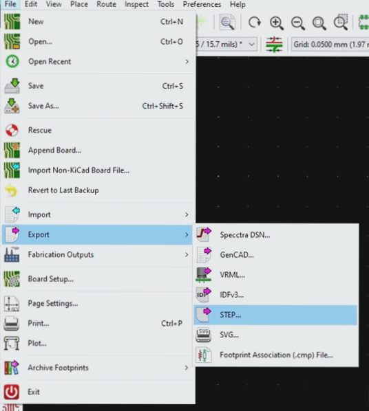
When you’re ready to export the PCB design to another CAD program, you have two main options. If you’ve already attached STEP files to your components in KiCad, exporting via the STEP format will be straightforward. This export will include the PCB layout along with each component’s 3D model. However, note that the exported STEP files will not include pad locations or silkscreen details. The image below illustrates the process of exporting via the STEP menu. This method generates individual STEP files for both the PCB and any components that have STEP files assigned, positioning the components correctly on the board, but without pads visible.
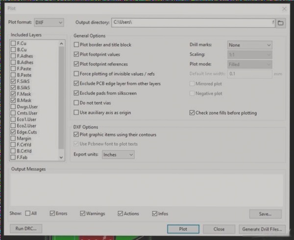
If you require pad locations and silkscreen layers in your export, you can export specific layers as a DXF file, which can then be imported into your CAD program to create parts and assemblies based on these layers. To do so, go to File → Plot, select DXF as the output format, and choose the layers you wish to export.
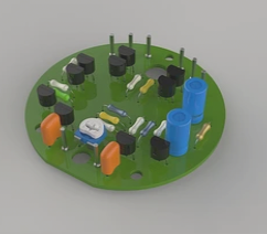
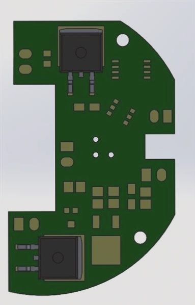
With these individual DXF files, you can create an extrusion to generate a new part containing all the PCB’s details (excluding the components themselves). Be aware that exporting circular geometries might cause issues, as circles will be represented as many small line segments. This could lead to problems when assembling the PCB, especially when using concentric mates in SolidWorks or other CAD programs. You can resolve this by editing the DXF in your CAD software, replacing line segments with a true circle. Additionally, you can combine this method with the STEP export to generate a more complete PCB model that includes electrical components. The image below shows the result of following these steps. Remember that any sharp corners in the PCB cut will be slightly rounded on the inner edges, so be sure to account for this in your design, especially if the PCB is intended to be press-fitted into a housing or mounting structure.
If you have any questions regarding PCB or PCBA, please feel free to contact me at info@wellcircuits.com.