Introduction
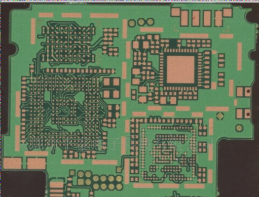
The purpose of PCB etching is to complete the circuit board after it has been electroplated and removed from the electroplating equipment. The post-processing includes several important steps:
1. Film Removal: The dry film used for anti-plating purposes is peeled off using a potion. The hardened dry film partially dissolves under the dope and partially peels off into flakes. The efficiency of the filtration system is crucial to maintain the effectiveness of the liquid and completeness of the post-washing.
2. Line Etching: This step involves dissolving the copper in the non-conductor part.
3. Stripping Tin and Lead: Finally, the etch-resistant tin-lead coating is removed. This step is necessary for processing and does not add any value. However, special attention is required to avoid defects in the completed outer layer circuit.
The typical PCB processing process currently follows the “pattern plating method. This involves pre-plating a lead-tin resist layer on the copper foil part that needs to be retained on the outer layer of the board, followed by chemical corrosion of the rest of the copper foil. It should be noted that there are two layers of copper on the board at this point. Therefore, the etching process must completely remove one layer of copper while the rest forms the final required circuit. Another process method is the “full board copper plating process”, which coats the entire board with copper and uses a tin or lead-tin resist layer only on the part other than the photosensitive film.
In the etching process, tin or lead tin is the commonly used resist layer, used with ammonia etchant. Sulfate-based etching solution can be separated by electrolysis and reused due to its low corrosion rate. The quality of etching requires complete removal of copper layers except under the resist layer while maintaining consistency of wire width and minimizing undercut. The etching factor, which measures the ratio of the width of side etching to the depth of etching, is an important parameter that needs to be controlled.
The quality of etching is influenced by the structure of the etching equipment and the etching solution composition. The use of certain additives can help reduce side etching. Additionally, problems with etching quality may originate in the stripping process, and the various processes in PCB processing are closely interconnected.
The ideal state in the etching process after electroplating should have the thickness of copper and tin or lead-tin not exceeding the thickness of the photosensitive film and the electroplating resistance. However, in actual production, the coating pattern is often thicker than the photosensitive pattern, leading to challenges such as residual glue and incomplete etching.
The formation of “copper roots” and deposits in the etching solution can also impact the efficiency and quality of the etching process. Therefore, maintaining high-quality etching is crucial for the successful production of PCBs.


