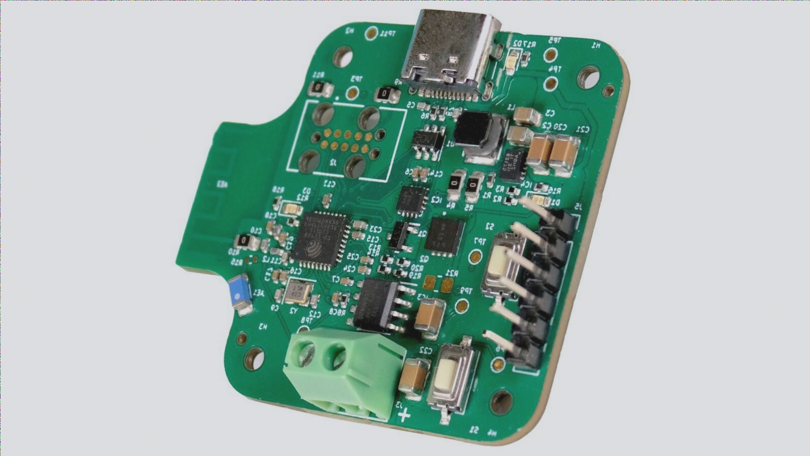
2. QFN solderability inspection and testing
Just like the BGA solder inspection standards, current solder inspection of QFN packages not only employs electrical testing to detect their functionality but also utilizes optical sensors or X-rays to inspect solder open and short circuits. Frankly, if the quality of X-Ray imaging is subpar, identifying soldering issues in QFN packages can be quite challenging. If troubleshooting solderability issues is imperative, resorting to destructive experiments such as slicing or inspecting BGA solder might be necessary.
3. Possible solutions for QFN air welding
When encountering voids in QFN solder joints, it’s essential to determine whether it stems from component oxidation. Conducting a solderability test on the component can confirm this, followed by investigating potential issues with specific solder joints. Typically, grounding joints are more prone to this phenomenon. To address void soldering, revising the circuit board’s wiring design is advisable. Introducing thermal resistance pads along the circuit board lines can reduce the prevalence of large areas of solder feet directly grounded, thereby mitigating heat dissipation. Thermal resistance involves narrowing the grounding circuit width to prevent immediate heat conduction to the entire grounded copper sheet. Adjusting furnace temperature or transitioning to a ramp-up reflow soldering curve can also mitigate the issue of solder paste absorbing excessive heat during preheating.
Excessive solder paste application on the ground pad at the center of the QFN’s bottom has been observed. During reflow soldering, this can cause parts to float, leading to void soldering issues. In such cases, reconsidering the ground pad’s design by employing a stencil with apertures rather than full coverage can be beneficial. This approach reduces the likelihood of parts floating due to excessive solder paste melting into a ball during reflow soldering. Furthermore, minimizing through holes on the circuit board’s solder pads and plugging the through holes on the central heat dissipation grounding pad whenever possible is advisable. Failure to do so may result in solder quantity discrepancies and bubble formation, potentially leading to poor soldering quality in severe instances.


