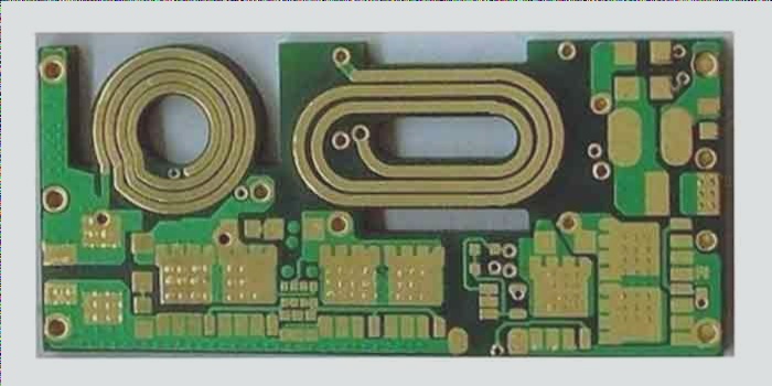
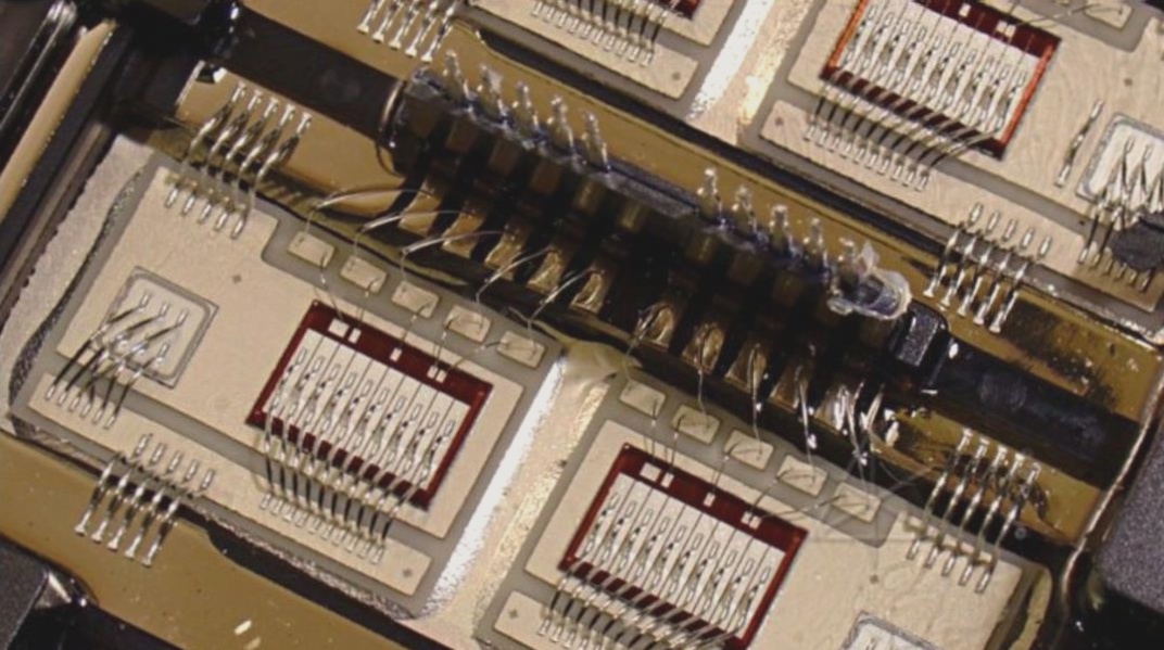
QFN (Quad Flat No Leads) is becoming increasingly popular in the electronics industry today for IC packaging. QFN offers several advantages such as small size similar to CSP (Chip Scale Package) and cost-effectiveness. The IC production process yield is high and it provides excellent coplanarity and heat dissipation capabilities for high-speed and power management circuits. Compared to traditional packaged ICs like SO packages, the QFN package does not require pins to be leaded out from four sides, resulting in better electrical performance.
Despite its benefits, the leadless design of QFN poses challenges for circuit board assembly factories in terms of soldering quality. Due to the difficulty in visually inspecting solder joints, it is tough to assess solderability. Some IC packaging companies expose the cut surface by cutting the lead-frame without electroplating, making it difficult to solder the sides of the QFN. The exposed surface may oxidize over time, further complicating the soldering process.
The IPC-A-610D (PQFN) specification does not clearly mandate a smooth arc-shaped curve for the side soldering of QFN. In other words, the focus should be on ensuring proper soldering at the bottom of the QFN and heat sink positions, rather than the side soldering. Soldering at the bottom of the QFN can be compared to BGA soldering, and reference can be made to IPC-A-610D Section 8.2.12 Plastic BGA standards. The soldering of the middle grounding pad may vary depending on individual company designs.
Similar to BGA solder inspection standards, inspecting QFN solder joints requires electrical measurements and optical sensors or X-ray scans to detect solder defects. If X-ray scans are insufficient, identifying soldering issues with QFN can be challenging. In case of solderability problems, destructive methods like slicing or examining BGA solder may be necessary.
If empty solder joints are detected in QFN, it is essential to determine if oxidation is the issue by conducting a solderability test. For empty soldering on grounding pads, consider altering circuit board wiring design or adding thermal resistance pads to reduce excessive heat dissipation. Adjusting furnace temperatures or using a ramp-up reflow profile can also prevent solder paste from absorbing too much heat.
To prevent floating issues during reflow soldering, avoid through-holes on solder pads and limit plugs on the middle grounding pad. Full-chip printing on the middle grounding pad can reduce the likelihood of floating parts caused by excessive solder melting. Avoiding through holes can prevent solder amount discrepancies and bubble formation, ultimately ensuring better soldering outcomes.


