What is the difference between PCB and PCBA
Many are familiar with PCB circuit boards, often encountered in daily life, but may not know much about PCBA and could confuse it with PCB. So, what exactly is a PCB? How did PCBA come to be? What distinguishes PCB from PCBA? Let’s delve deeper into these topics.
About PCB
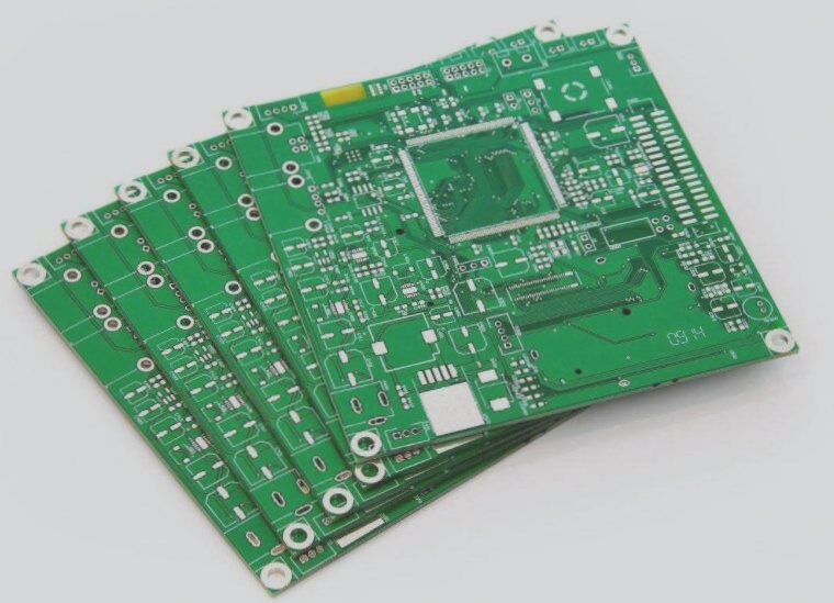
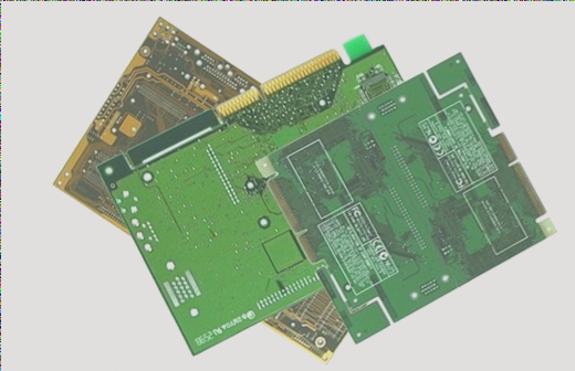
PCB stands for Printed Circuit Board, which in Chinese is translated as “printed circuit board.” This name comes from its manufacturing process involving electronic printing. PCBs are crucial electronic components in the electronics industry, serving as a support for electronic components and a medium for electrical connections. They are widely utilized in electronic product manufacturing. The key characteristics of PCBs can be summarized as follows:
1. High wiring density, compact size, and lightweight, all of which facilitate the miniaturization of electronic devices.

2. Thanks to the repeatability and consistency of the graphics, wiring and assembly errors are minimized, resulting in reduced maintenance, debugging, and inspection time for the equipment.
3. This process promotes mechanization and automation in production, enhancing labor productivity and lowering the costs associated with electronic equipment.
4. The design can be standardized to enable interchangeability.
**About PCBA**
PCBA stands for Printed Circuit Board + Assembly, indicating that PCBA undergoes the entire manufacturing process, including PCB blank board SMT and then DIP insertion. The basic processing steps for PCBA are:
1. **Single-sided surface assembly process:** solder paste printing → component placement → reflow soldering;
2. **Double-sided surface assembly process:** A-side solder paste printing → component placement → reflow soldering → flip board → B-side solder paste printing → component placement → reflow soldering;
3. **Single-sided mixed assembly (SMD and THC on the same side):** solder paste printing → component placement → reflow soldering → manual insertion (THC) → wave soldering;
4. **Single-sided mixed assembly (SMD and THC on both sides of the PCB):** B-side red glue printing → component placement → red glue curing → flip → A-side insertion → B-side wave soldering;
5. **Double-sided mixed assembly (THC on side A, SMD on both sides A and B):** A-side solder paste printing → component placement → reflow soldering → flip board → B-side red glue printing → component placement → red glue curing → flip board → A-side insertion → B-side wave soldering;
6. **Double-sided mixed packaging (SMD and THC on both sides A and B):** A-side solder paste printing → component placement → reflow soldering → flip board → B-side red glue printing → component placement → red glue curing → flip board → A-side insertion → B-side wave soldering → B-side insertion completed.
Note: SMT and DIP are both methods for integrating components onto the PCB. The key difference is that SMT does not require drilling holes in the PCB, while DIP involves inserting component pins into pre-drilled holes.
SMT (Surface Mount Technology) primarily utilizes mounters to attach small components to the PCB. The production sequence includes: positioning the PCB, solder paste printing, mounting with mounters, reflow soldering, and final inspection.
DIP refers to “dual in-line package,” meaning that components are inserted onto the PCB. This method is suitable for larger components that are not compatible with surface mount technology. The main production steps are: applying adhesive, inserting components, inspecting, wave soldering, and final inspection.
**The Difference Between PCB and PCBA**
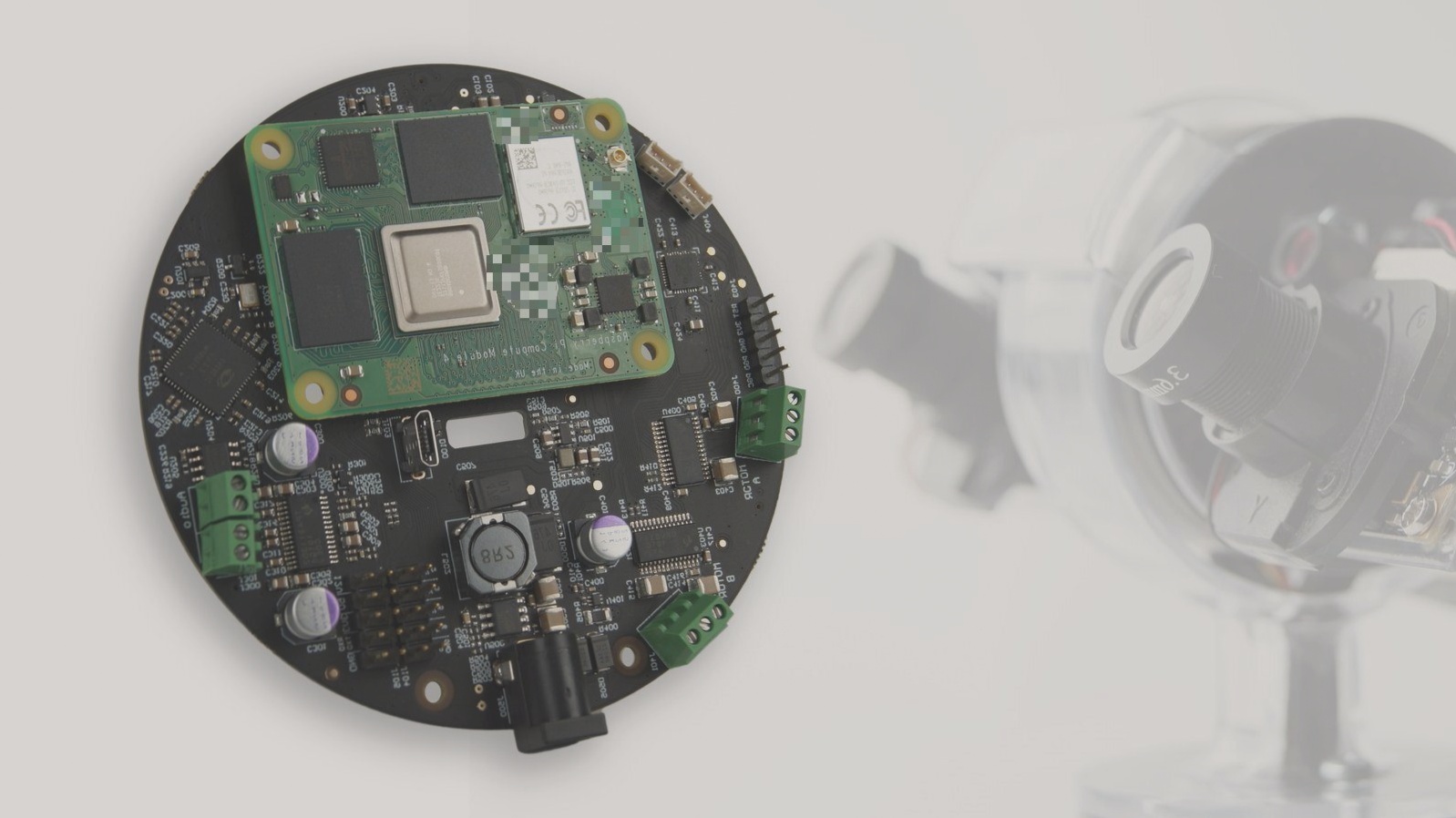
As outlined above, PCBA generally refers to a processing method and can also be viewed as a completed circuit board, meaning that PCBA is recognized once all processes on the PCB are finished. In contrast, PCB refers to an unpopulated printed circuit board without any components.
In summary: PCBA is a finished board; PCB is a bare board.
Many are familiar with PCB circuit boards, often encountered in daily life, but may not know much about PCBA and could confuse it with PCB. So, what exactly is a PCB? How did PCBA come to be? What distinguishes PCB from PCBA? Let’s delve deeper into these topics.
About PCB
PCB stands for Printed Circuit Board, which in Chinese is translated as “printed circuit board.” This name comes from its manufacturing process involving electronic printing. PCBs are crucial electronic components in the electronics industry, serving as a support for electronic components and a medium for electrical connections. They are widely utilized in electronic product manufacturing. The key characteristics of PCBs can be summarized as follows:
1. High wiring density, compact size, and lightweight, all of which facilitate the miniaturization of electronic devices.
2. Thanks to the repeatability and consistency of the graphics, wiring and assembly errors are minimized, resulting in reduced maintenance, debugging, and inspection time for the equipment.
3. This process promotes mechanization and automation in production, enhancing labor productivity and lowering the costs associated with electronic equipment.
4. The design can be standardized to enable interchangeability.
**About PCBA**
PCBA stands for Printed Circuit Board + Assembly, indicating that PCBA undergoes the entire manufacturing process, including PCB blank board SMT and then DIP insertion. The basic processing steps for PCBA are:
1. **Single-sided surface assembly process:** solder paste printing → component placement → reflow soldering;
2. **Double-sided surface assembly process:** A-side solder paste printing → component placement → reflow soldering → flip board → B-side solder paste printing → component placement → reflow soldering;
3. **Single-sided mixed assembly (SMD and THC on the same side):** solder paste printing → component placement → reflow soldering → manual insertion (THC) → wave soldering;
4. **Single-sided mixed assembly (SMD and THC on both sides of the PCB):** B-side red glue printing → component placement → red glue curing → flip → A-side insertion → B-side wave soldering;
5. **Double-sided mixed assembly (THC on side A, SMD on both sides A and B):** A-side solder paste printing → component placement → reflow soldering → flip board → B-side red glue printing → component placement → red glue curing → flip board → A-side insertion → B-side wave soldering;
6. **Double-sided mixed packaging (SMD and THC on both sides A and B):** A-side solder paste printing → component placement → reflow soldering → flip board → B-side red glue printing → component placement → red glue curing → flip board → A-side insertion → B-side wave soldering → B-side insertion completed.
Note: SMT and DIP are both methods for integrating components onto the PCB. The key difference is that SMT does not require drilling holes in the PCB, while DIP involves inserting component pins into pre-drilled holes.
SMT (Surface Mount Technology) primarily utilizes mounters to attach small components to the PCB. The production sequence includes: positioning the PCB, solder paste printing, mounting with mounters, reflow soldering, and final inspection.
DIP refers to “dual in-line package,” meaning that components are inserted onto the PCB. This method is suitable for larger components that are not compatible with surface mount technology. The main production steps are: applying adhesive, inserting components, inspecting, wave soldering, and final inspection.
**The Difference Between PCB and PCBA**
As outlined above, PCBA generally refers to a processing method and can also be viewed as a completed circuit board, meaning that PCBA is recognized once all processes on the PCB are finished. In contrast, PCB refers to an unpopulated printed circuit board without any components.
In summary: PCBA is a finished board; PCB is a bare board.

