Advancements in PCB Technology
In recent years, the evolution of smartphones and tablets has driven significant advancements in computer technology. These devices continue to improve in performance, storage capacity, and battery life with each iteration. This progress is largely due to innovations in semiconductor technology, 3D ICs, high-end heterogeneous packaging, and upgrades in PCB carrier technology.
The Role of PCBs in Electronics
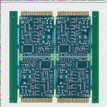
Printed circuit boards (PCBs) play a crucial role in supporting electronic components and creating conductive pathways. PCB manufacturing involves insulating carrier boards, with the choice of materials impacting strength, insulation properties, and electrical performance. Conductive pathways can be created using additive or subtractive methods.
Key Points in PCB Manufacturing:
- Testing precision in manufacturing and chemical processing is crucial for single-layer, double-layer, and multi-layer designs.
- Multi-layer PCBs reduce substrate size, accommodating the integration of complex circuits and components.
- High-density PCBs offer profitability but require intricate design and testing processes.
- Optimizing substrate materials and metal layers is essential for stability and thermal resistance.
- Finishing processes like plating enhance PCB durability, while epoxy resin protects against moisture-induced warping.
Challenges and Considerations:
- The choice of metal layer material significantly impacts electrical properties.
- Complex testing and verification are necessary for high-density multi-layer boards.
- Managing material temperature variations ensures stability and design specifications adherence.
- Protecting against issues like oxidation and copper foil peeling is crucial for PCB longevity.
Conclusion
As electronic products demand higher precision and complexity, PCB technology continues to advance, offering improved performance and efficiency while requiring meticulous attention to material selection, design, and testing processes.
PCB Manufacturing Process Best Practices
- After completing the circuit board assembly, it is crucial to add an anti-oxidation layer to the metal surfaces requiring tin adhesion. This can be achieved through methods such as Hot-Air Solder Leveling (HASL), Electroless Nickel/Immersion Gold (ENIG), Immersion Silver (ImAg), Immersion Tin, or Organic Solderability Preservatives (OSP) to ensure protection.
- Verification of finished circuit boards is essential due to the various checkpoints involved in the manufacturing process. Regular maintenance and cleaning of process equipment are necessary to maintain stable production conditions in a high-cleanliness environment, reducing errors in the final product.
- Board processing includes multiple chemical liquid immersion operations that require equipment to maintain automatic temperature, timing, and fixed-speed processing. Chemicals should be added based on the liquid’s pH to ensure stability.
- Standardized manufacturing processes are vital for product quality, emphasizing the need for a clean environment to prevent contamination.
- Production lines should operate in dust-free environments, and liquid photoresist production must include dust filtering and board surface cleaning conditions to maintain quality standards.
- Throughout production, consistent attention is required at all stages to uphold quality and minimize defects in the back-end workpieces.
- Quality issues during each PCBA processing section must be addressed promptly as defects can have a significant impact on the final product quality.
- Each manufacturing stage necessitates initial product testing, final product testing, and intermediate sampling to ensure quality supervision during PCBA processing.
- Drilling processes can utilize pin gauges to verify hole diameter and ensure initial product quality. Electroplating can use palm-type gauges to check copper thickness and density for plated holes.
- After copper plating, it is essential to remove any glass fiber, resin, or dust and level the copper surface using an abrasive belt machine.
- In high-volume production, machine vision systems aid in inspecting workpieces, while X-ray technology confirms inter-layer alignment accuracy.
- Automatic optical inspection can compare circuit drawings to identify potential issues such as disconnections, short circuits, or gaps.
- During the solder mask process, pickling, brushing, and microetching bare copper are essential steps to remove oxide layers and micro copper particles, enhancing surface roughness for improved ink adhesion.
- In the printing stage, visual inspection of ink uniformity is crucial. After baking, the thickness of the coated ink should be measured using a film thickness meter.
- Pressing multi-layer boards effectively relies on temperature and pressure control. A two-stage process can extend hot pressing time to enhance the board’s hardness, flatness, and copper foil adhesion.
- Final product verification of the circuit board can be facilitated through CAM Data, utilizing automatic fixture software to create production programs for quick detection and selection of defective workpieces.