
Printed Circuit Board Industry Trends and Characteristic Impedance Control
Our country’s economy is thriving with a focus on economic construction, reform, and opening up. The electronic industry is experiencing rapid growth, with the printed circuit board (PCB) sector following suit. As the world undergoes technological and industrial changes, PCBs play a crucial role in the development of electronics, especially with the increasing demands for miniaturization, digitization, high frequency, and multi-functional electronic devices.
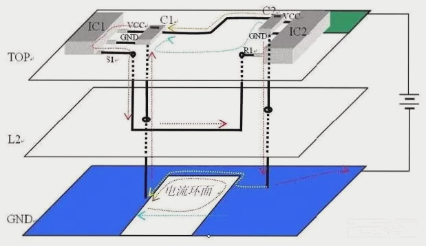
For PCBs used in high-frequency and high-speed digital signal transmission, ensuring circuit continuity, absence of short circuits, and meeting characteristic impedance requirements are essential for optimal performance.
Importance of Characteristic Impedance in PCBs
Characteristics impedance control in PCBs is vital for preventing signal reflections, maintaining signal integrity, reducing transmission loss, and facilitating impedance matching. This is particularly crucial in surface microstrip structure multilayer boards.
Surface Microstrip Line and Characteristic Impedance
The surface microstrip line, known for its relatively high characteristic impedance, is commonly used in PCB designs. It consists of a signal line surface separated from a reference plane by insulating materials.
- Microstrip Z Formula: Z = (87 / √(Er+1.41)) (ln[5.98H / (0.8W+T)])
- Stripline Z Formula: Z = (60 / √Er) (ln[4H / (0.67π(0.8W+T)])
Factors such as dielectric constant (Er), dielectric thickness (H), wire width (W), and wire copper thickness (T) significantly impact characteristic impedance. Proper substrate material selection is crucial in PCB design to ensure optimal characteristic impedance performance.

 العربية
 简体中文
简体中文 Nederlands
 English
 Français
 Deutsch
 Italiano
 日本語
日本語 한국어
한국어 Português
 Русский
 Español
 ไทย
ไทย