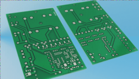
Understanding Multilayer PCBs
Products with three or more layers are known as multilayer PCBs, allowing for a higher density of components compared to traditional double-sided boards. The use of multiple layers is essential due to space limitations on a single layer.
Evolution of PCB Layers
Originally, four-layer PCBs were common but have now evolved to six or more layers to support high-density assembly requirements.
Production Process Overview
- Print and Etch: Involves processes like alignment, image transfer, etching, and stripping.
- Post-etch Punch: Includes copper treatment, etching, and tool hole creation.
- Drill and Panel-plate: Encompasses drilling, plating, etching, and stripping.
Material Preparation Considerations
Attention to detail is crucial during material preparation, including cutting methods, edging considerations, and dimensional stability through baking.
Copper Surface Treatment
Copper surface treatment plays a vital role in the PCB manufacturing process, impacting subsequent steps. Various treatment methods are employed, such as brushing, sandblasting, and chemical methods.
Brushing Method
- Ensuring uniform brush wheel usage for even surface height.
- Conducting brush mark experiments to assess depth and uniformity.
- Advantages:
- Low cost
- Simple manufacturing process
- Disadvantages:
- Challenges with thin circuit boards
- Unsuitable for inner layers
- Potential for adhesion issues and infiltration
Sandblasting Method
- Utilizing fine stones like pumice for abrasion.
- Benefits include superior roughness and stability.
- Disadvantages:
- Adherence of pumice to surfaces
- Machine maintenance challenges
Chemical Method (Microetching)
This method provides detailed information on image transfer and printing techniques used in conjunction with microetching.