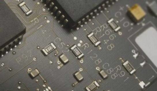
Additionally, VLP and LP copper foil possess the following features beyond the general performance of regular copper cylinders:
- The initial precipitation of VLP and LP copper foil forms a crystalline layer with a certain distance, preventing sliding between metal grains. This robust structure provides greater resistance against deformation from external conditions, resulting in better tensile strength and elongation (normal state and thermal state) compared to general electrolytic copper foil.
- LP copper foil has a smoother and finer roughened surface than ordinary copper foil, preventing residual copper powder (copper powder transfer phenomenon) after etching. This enhances the surface resistance and interlayer resistance characteristics of the PCB and improves the reliability of dielectric properties.
- It exhibits high thermal stability, preventing copper recrystallization on thin substrates from multiple laminations.
- LP copper foil reduces etching time for graphic circuits and side erosion, as well as decreasing white spots after etching, making it suitable for fine line production.
- It possesses high hardness, improving the drillability of multilayer boards and is suitable for laser drilling.
- LP copper foil maintains a relatively flat surface after pressing and forming multilayer boards, ideal for the production of fine line circuits.
- The uniform thickness of LP copper foil results in low signal transmission delay after PCB production, well-controlled characteristic impedance, and reduced noise between lines and layers.
The low-profile copper foil manufacturing technology has made significant improvements and technological advancements in terms of microstructure, such as grain size, distribution, and crystal orientation.
In addition, ultra-thin copper foil is essential for multilayer boards with micro-buried and blind vias, as well as for organic resin packaging substrates for portable electronic products. The CO2 laser etching process also demands ultra-thin copper foil as the substrate material to directly process micro-holes. Countries like Japan and the United States have industrialized the production of 9μm, 5μm, and 3μm electrolytic copper foil. However, the production of ultra-thin copper foil faces two main technical challenges: ensuring a high product qualification rate during direct production from the carrier, and developing a new type of ultra-thin copper foil carrier. Some manufacturers have developed a film-type carrier, offering advantages of lightweight, easy access, and good peelability after plate forming and pressing.

