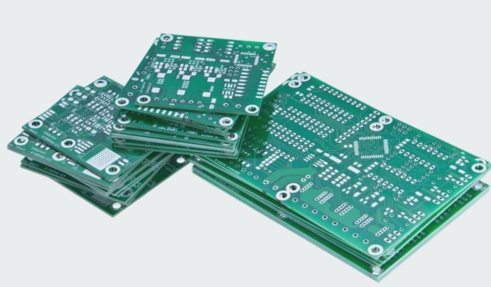
Introduction:
As the wiring density of flexible substrates increases, circuits produced by the traditional subtractive process can no longer meet the demands for finer circuit features. As a result, the industry is increasingly adopting semi-additive manufacturing processes. Additionally, advanced technologies for producing thin and embedded flexible substrates are being progressively utilized for mass production.
Electrodeposition Polyimide Process:
The protective layer for flexible substrate circuits is typically formed using a “binder + polyimide” combination or specialized flexible substrate inks. However, in recent years, the electrodeposition polyimide process has emerged as an alternative. This process deposits a protective layer specifically around the circuit, as shown in Figure 4 for a comparison of these three methods.

Advantages of the Electrodeposition Polyimide Process:
-
1) High Circuit Density: The binder-polyimide film used for circuit protection can struggle to adhere properly to the substrate, potentially leaving gaps. In contrast, the electrodeposition process forms an independent electrochemical layer that tightly encases the circuit, ensuring effective protection for high-density circuits.
-
2) Adaptation to High-Frequency Requirements: Conventional films or inks form a continuous protective layer, which may influence the dielectric constant based on material properties. The electrodeposited polyimide, however, forms a protective layer around the circuit, creating an “air layer” between two protective layers, which is ideal for high-frequency applications.
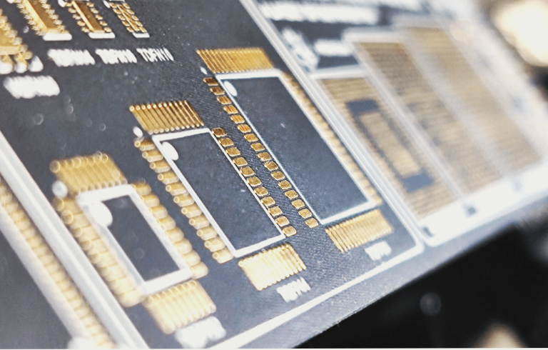
Etching Process in the Electrodeposition Polyimide Process:
Traditional polyimide hole processing methods rely on mechanical or laser punching and drilling. However, electroless etching technology offers a more advanced approach for flexible substrates. This process uses an alkaline solution to degrade the imide bonds, triggering a hydrolysis reaction that breaks the imide ring. The resulting low-molecular compounds dissolve in the solution, allowing precise etching to create the desired holes.

The main process flow is outlined below:
-
1) Graphic Transfer Technology: Copper foil is removed from the hole positions to define the hole sites.
-
2) Polyimide Etching: A specialized polyimide etching solution is used to etch the substrate.
-
3) Electroless Plating: Electroless plating or PTH (Plated Through Hole) processes are applied to the etched hole sites.
In comparison to traditional methods, the etching process can handle all hole formations in a single operation, reducing both time and cost irrespective of the number of holes. For example, with a 25µm PI film, the minimum hole diameter can reach 35µm, similar to YAG laser drilling capabilities. Additionally, because all hole sites are defined at once using optical imaging, the positioning accuracy of the holes is significantly improved to meet the high-density requirements of flexible substrates. Localized etching of polyimide to create air-displaced spaces can also reduce capacitance between circuits, mitigating issues like RC delay, cross-talk, and resonance frequency drops, thereby enhancing high-speed signal transmission.
If you have any questions about PCB and PCBA, please feel free to reach out to me at info@wellcircuits.com.