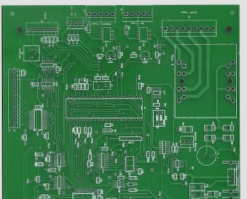
A quick question about v-scored panels (no routing/milling):
Should each separate PCB outline (“Dimension” in Eagle-speak) be included with the panel along with the outer panel outline? Or should the individual outlines be removed when adding them to an exclusively v-scored panel?
From looking around it looks like it’s done both ways. There’s too much English in my question for the fab to answer coherently.
I ask because Eagle cuts out dimensions-within-dimensions (with Board Shape Detection enabled) and it looks funny, and I don’t know if the individual PCB dimensions are used for anything at the fab for these types of panels. Sample in first picture.
Which layer should the V-Score line be on (I used the Eagle default 102)? Where should that layer be included in the Gerbers? Should it be annotated on that layer (as shown in the second picture)?


