
Transitioning to SMT PCB Design: Challenges and Considerations
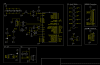
As I venture into the realm of Surface Mount Technology (SMT) PCB design, I find myself faced with new challenges and considerations. My current project necessitates the use of the TQFP package for the atmega32u4, pushing me out of my comfort zone with through-hole designs. The task at hand involves connecting two OLED screens via SPI, one operating at 5V and the other at 3.3V, facilitated by a 4050 level shifter.
Initially aiming for a 10MHz SPI bus speed, practical testing has led me to operate at a more conservative 2.5MHz. The 3.3V display interfaces directly with the PCB through a 2×8 header, while the 5V display is linked via a short 10cm ribbon cable.
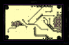
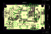
Upon reviewing my layout, I noticed a potential concern near U2, where a portion of the ground plane relies solely on a pin connection to the atmega. To address this issue and optimize the design for performance, I am contemplating revisiting the layout to enhance connectivity and possibly relocate the ground plane to the bottom layer.
Having predominantly worked with lower-speed through-hole designs in the past, navigating the intricacies of high-speed SMT PCB layout poses a learning curve that I am eager to overcome.
 العربية
 简体中文
简体中文 Nederlands
 English
 Français
 Deutsch
 Italiano
 日本語
日本語 한국어
한국어 Português
 Русский
 Español
 ไทย
ไทย