Immersion Gold (ENIG)
- ENIG’s Protection Mechanism:
- Ni/Au Chemical Process:
- Immersion Gold Process:
- ENIG Advantages:
- Limitations of ENIG:
- Chemical Immersion Silver:
- Electroplating Nickel Gold:
- PCB Hybrid Surface Treatment Technology:
- Hot Air Leveling:
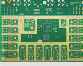
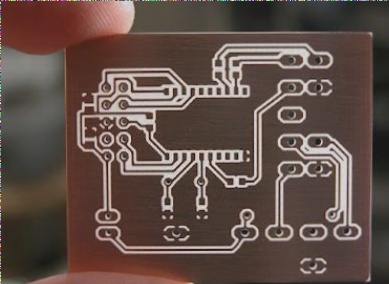
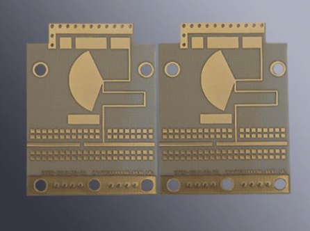
ENIG involves applying a thick layer of nickel-gold alloy on the copper surface, providing long-term protection for the PCB. Unlike OSP, which only acts as an anti-rust barrier, ENIG enhances PCB longevity and ensures superior electrical performance. Additionally, ENIG offers environmental resistance that sets it apart from other surface treatments.
In the ENIG process, nickel and gold are chemically deposited onto the copper surface. The nickel layer acts as a barrier between the solder and copper, while the gold layer prevents oxidation or passivation during storage. The thickness of the nickel layer is typically 120 to 240 μin, while the gold layer is thinner at 2 to 4 μin.

In immersion gold, a thin, continuous gold protective layer is deposited on the PCB surface. This layer must not be too thick to avoid making solder joints brittle. Immersion gold offers high strength, abrasion resistance, and oxidation resistance, making it suitable for high-strength applications.
ENIG-treated PCB surfaces are flat with excellent coplanarity, ideal for contact surfaces like buttons. The process provides excellent solderability, with the gold quickly dissolving into the molten solder.
The ENIG process is complex and requires precise control of parameters to avoid issues like black pads, which can impact solder joint reliability. Excessive oxidation of nickel and gold can lead to black pad formation.
This simpler and faster process maintains good electrical performance and solderability. However, the lack of a nickel layer reduces physical strength compared to ENIG.
This method involves electroplating nickel and gold layers on the PCB surface to prevent diffusion between gold and copper. Two types of electroplated nickel gold are soft gold (used for wire bonding) and hard gold (used for non-soldered electrical interconnections).
This approach combines two or more surface treatment methods to enhance PCB performance. Common combinations include Immersion Nickel Gold + Anti-oxidation and Electroplating Nickel Gold + Hot Air Leveling.
Hot air leveling is a cost-effective surface treatment method that complies with EU RoHS regulations. It is commonly used for PCB surface finishing.
RoHS Directive: Enhancing Environmental Protection in PCB Manufacturing
The RoHS Directive, short for “Restriction of Hazardous Substances,” is a crucial regulation introduced by the European Union to ensure the safety of electronic and electrical PCB products. Enforced since July 1, 2006, this directive sets forth stringent material and process guidelines aimed at safeguarding human health and the environment.
One of the primary objectives of the RoHS Directive is to phase out the usage of six hazardous substances in PCB manufacturing. These substances include lead, mercury, cadmium, hexavalent chromium, polybrominated biphenyls, and polybrominated diphenyl ethers. Notably, the directive specifies that the lead content in PCBs must not exceed 0.1%, underscoring the commitment to reducing environmental impact and promoting sustainable practices.
- Established by EU legislation, the RoHS Directive plays a pivotal role in enhancing environmental protection standards within the PCB industry.
- By restricting the presence of hazardous substances, such as lead and mercury, the directive contributes to safer manufacturing processes and promotes eco-friendly technologies.
- Compliance with the RoHS Directive is essential for manufacturers seeking to uphold quality, sustainability, and regulatory requirements in the production of electronic components.


