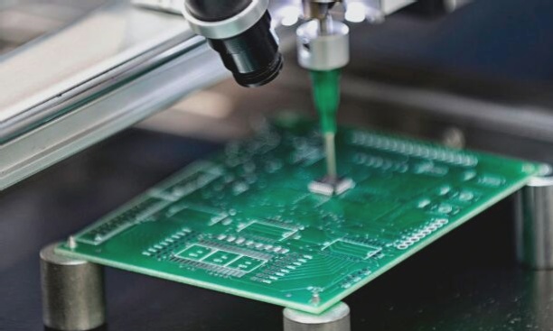
IEC 6118 Standard for PCB Pad Shapes
The International Electrotechnical Commission (IEC) has established the IEC 6118 standard to address the varying requirements for solder fillet or pad bump conditions on printed circuit boards (PCBs). This standard offers two key methods for defining PCB pad shapes:
- Method 1: This method involves precise data derived from industrial component specifications, PCB fabrication processes, and component placement accuracy capabilities. Each pad shape is specific to a particular component and is identified by a corresponding number.
- Method 2: The second method utilizes specific equations to adapt the provided information for a more robust solder connection. This approach is particularly valuable in situations where equipment accuracy differs from the assumed values during pad design.
The standard categorizes PCB pad conditions into maximum, medium, and minimum material states for mounting various pins or component terminals. By default, these conditions are labeled as “desired targets” one, two, or three.

Pad Geometry Levels:
Level 1: Designed for low-density PCB applications, the “maximum” pad condition suits wave or flow soldering of leadless chip components and leaded fin components. This geometry also accommodates inward “T”-shaped pin components, offering flexibility for manual and reflow soldering processes.
Level 2: Intended for medium component density products, the “medium” pad geometry aligns closely with the IPC-SM-782 standard. These pads ensure robust soldering conditions for reflow soldering processes and are suitable for various component types.
Level 3: Tailored for high component density products, such as portable devices, the “minimum” pad geometry may be utilized. However, not all products may be suitable for the smallest land shape. Prior to implementation, thorough testing based on specific product requirements is recommended.
The pad geometries specified in IPC-SM-782 and IEC61188 are designed to accommodate PCB component tolerances and process variations. While IPC standard pads are suitable for most assembly applications, certain companies may require minimal pad geometries for high-density applications, like portable electronics.
The IEC61188 international PCB land standard caters to applications with higher part density, offering guidance on land geometry for specific product categories. This information ensures the correct size, shape, and tolerances of surface mount pads, facilitating proper soldering fillets, inspection, testing, and rework of solder joints.