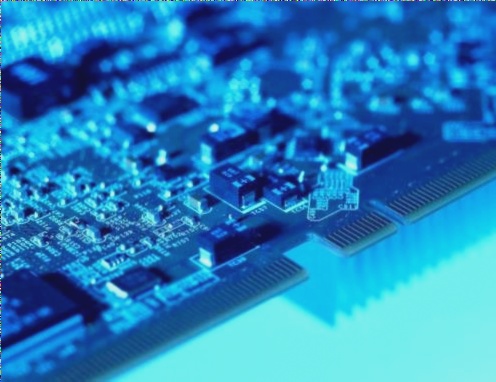
Advanced Technologies in High-Density PCB Production
High-density PCB circuit boards are characterized by very small line widths and line spacings, requiring advanced production technologies for optimal results.
Fine Line Production Technology
- Traditional machines struggle to achieve lines below 4 mil, leading to the development of advanced DES technology.
- Research is focused on achieving 3mil/3mil, 2mil/3mil, and 2mil/2mil line width and spacing.
Thermosetting Ink Lamination Technology (TCD Technology)
TCD technology revolutionizes the creation of the SBU layer in HDI boards by using electroless copper deposition after silk-screen thermosetting ink, offering several advantages:
- Adjustable Dielectric Thickness: Users can customize dielectric thickness by using thicker thermosetting ink, providing flexibility in design.
- Easy Laser Drilling: The resin-based ink simplifies laser drilling, requiring lower and more stable energy levels than traditional materials.
- Reduced Manufacturing Costs: Elimination of expensive semi-cured resin with glass cloth leads to significant cost savings.
- Simplified Production Process: TCD technology allows for direct laser drilling after ink printing, streamlining the manufacturing process.
These advanced technologies are shaping the future of high-density PCB production, offering improved efficiency and cost-effectiveness.