Understanding PCB Types and Their Advantages
- Single-Side PCB vs. Double-Side PCB
- Color Varieties of PCBs
- Advantages of Multi-Layer Boards
- High assembly density and small volume
- Improved signal transmission speed
- Convenient wiring
- Enhanced shielding effect
- Challenges of Multi-Layer Boards
- Understanding FPC Flexible Circuit Boards
- Exploring Different PCB Layer Configurations
- Through Hole Design in PCBs
Single-side PCBs have components on one side and wires on the other, while double-side PCBs allow wiring on both sides, making them suitable for more complex circuits.
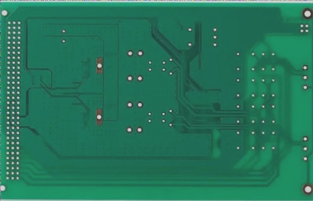
PCB boards are commonly green, but can also come in red, white, blue, yellow, black, purple, or light green, with each color serving different purposes in product grading.
While multi-layer boards offer numerous benefits, they also come with higher costs, longer processing cycles, and more complex quality detection procedures.
FPC flexible circuit boards can bend, which is both an advantage and a disadvantage, as bending can lead to copper foil circuit breakage. WellCircuits Co., Ltd. specializes in FPC production with advanced equipment and experienced teams.
PCBs can have varying layer configurations, from four or six layers commonly used in computer board cards to over 100 layers in practical printed circuit boards.
The design of through holes in PCBs is crucial, with considerations for hole structure, pad area, and isolation area, which are categorized as blind holes, buried holes, and through holes.
When designing high-speed PCBs, attention to parasitic capacitance and inductance in through-hole design is essential for optimal circuit performance.
Improving PCB Reliability with Advanced Technology
As the size of pads and through holes in PCBs continues to decrease, maintaining the right proportion with the plate thickness is crucial. A higher aspect ratio of the through hole can lead to reduced reliability. Thanks to advancements in laser drilling and plasma dry etching technologies, non-perforating small blind holes and buried holes are now possible.
By using non-perforating guide holes with a diameter of 0.3mm, the parasitic parameters introduced are only about 1/10 of those in traditional holes. This significant reduction enhances the overall reliability of the PCB.
The PCB Manufacturing Process
PCB manufacturing starts with a substrate made of GlassEpoxy resin or a similar material. The initial production step involves outlining the on-line wiring between components. This is achieved by printing the circuit negative of the designed PCB onto the metal conductor through negative transfer printing.