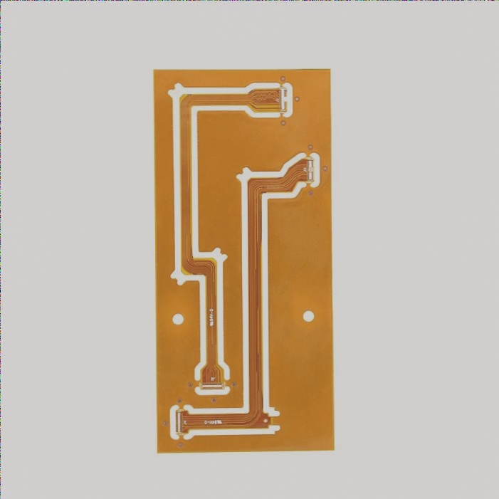
1. What is a build-up multi-layer board (BUM-PCB)?
2. Build-up Multilayer PCB (BUM) refers to an insulation substrate, similar to traditional double-sided or multi-layer boards, coated with an insulating medium. Electroless copper plating and copper electroplating are then utilized to form wires, while connection holes are overlaid multiple times to accumulate and create the required number of multilayer printed boards.
3. As early as the 1970s, BUM technology was documented in literature. However, it wasn’t until the early 1990s that the Japanese branch of IBM (Yasu) developed a photosensitive resin coating on the core board. The photoinduced method was employed to form the interconnections of vias.
4. The breakthrough came with the additive method, enabling the successful integration of this new wiring technology into Thinkpad notebook computers. This advancement was first published in 1991, termed Surface Laminar Circuit (SLC) due to its creation of unprecedented High-Density Interconnect (HDI) capabilities.
5. Japanese electronics manufacturers embraced this technology, marking the onset of the BUM era in PCB history.
6. BUM adapts to the requirements of electronic products for lighter, smaller, thinner, and shorter designs, catering to the needs of new-generation electronic packaging technologies such as BGA, CSP, MCM, and FCP. Consequently, its adoption surged throughout the 1990s, predominantly in portable electronic products like laptops, mobile phones, digital cameras, and MCM packaging substrates.
7. By 1998, the global BUM microplate market reached $1.1 billion, climbing to nearly $2 billion in 1999, with 90% of the market concentrated in Japan. By 2000, the market neared $3 billion. Domestic experts predicted a continued growth trajectory for the global BUM board market.
8. Presently and in the coming years, technological advancements and market competition in the PCB industry will center around BUM boards and its ancillary sectors such as materials, equipment, and testing.
9. Corresponding to Japan’s introduction of BUM (Multilayer Multilayer Board), European and American countries later proposed HDI (High-Density Interconnect). Essentially, these terms convey the same conceptual connotation.
10. According to IPC data, HDI is defined by non-mechanical drilling with a diameter less than 0.15mm (6mil), predominantly comprising blind holes (buried holes), and annular ring, pad, or land diameters less than 0.25mm (6mil). Holes meeting these criteria are termed micromovias.
11. PCBs with micromovias boast a contact density of 130 points/inch² or more, and a wiring density (with a channel width set at 50mil) exceeding 117 inches/inch². These are classified as HDI PCBs, with a line width/line spacing (L/S) of 3mil/3mil or less.
12. This underscores that the defining characteristic of build-up multi-layer boards is high-density interconnection (HDI).

