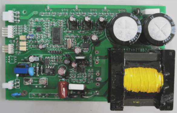
Common DFM Problems in PCB Design and How to Avoid Them
- Selection and Placement of Components
- Acute Angle
- Brass Bars and Isolated Islands
- A Tin Bridge Between Pins
- The Radiator
- Package Size According to IPC Standards
Designers often face challenges with in-line devices and their placement on the board. It is crucial to place components close together to avoid issues with soldering processes.
Sharp angles on copper elements can lead to acid buildup during PCB creation. Engineers should avoid acute angles near pads and aim for 45 or 90-degree angles to prevent this.
Copper bars and islands can cause problems in acid tanks, leading to short circuits or interference. Manual checks or software are essential to address this issue.
Proper solder resistance layers are critical to prevent solder bridges between pins, which can result in short circuits. Engineers must ensure alignment between pads and etching lines.
Managing heat sinks is crucial to prevent devices from floating off pads due to excessive solder paste. Dividing solder layer openings can help avoid short circuits during assembly.
Adhering to IPC standards for package design ensures reliable soldering during production, leading to cost-effective and high-quality products. Proper DFM implementation streamlines design and production processes, improving efficiency and reducing costs.
DFM plays a vital role in aligning design and production departments, facilitating information exchange, and optimizing production processes. By following standardized practices, companies can enhance automation, boost production efficiency, and minimize unnecessary investments in production test equipment. Implementing DFM not only enables smoother manufacturing processes but also fosters global product production, enhancing overall operational efficiency and competitiveness in the market.
The Importance of Design for Manufacturability (DFM) in PCB Design
Design for Manufacturability (DFM) plays a crucial role in ensuring the smooth production of PCBs. Without proper DFM specifications, assembly problems may arise during the late stages of product development or even in mass production. Addressing these issues through design changes at a later stage can significantly increase development costs and prolong the production cycle.
Therefore, prioritizing DFM alongside functionality is essential in the process of new product development. By incorporating DFM principles from the outset, manufacturers can streamline the production process, minimize errors, and ultimately reduce costs.
Latest Trends in DFM for PCB Design
- Integration of AI algorithms to optimize DFM processes
- Emphasis on collaboration between design and manufacturing teams
- Utilization of advanced simulation tools for DFM analysis
- Focus on eco-friendly and sustainable manufacturing practices


