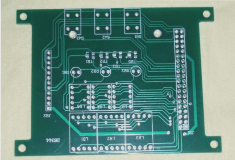
Crafting Multilayer Circuit Boards
When it comes to PCBs, circuits with more than two layers fall under the category of multilayer circuit boards. This implies that a minimum of three layers is required for a board to be considered multilayer. The process of laminating these layers together is crucial for the creation of multi-layer boards.
Ensuring Air-Free Layers
It is essential to prevent any air from being trapped between the layers of the PCB. The utilization of Eagle circuit board design software plays a vital role in the production of multilayer boards.
The Complex Process
The manufacturing process is intricate and typically commences with the preparation of a schematic diagram. Subsequently, the schematic is modified using the editor menu within the Eagle software.
Uniformity in Layers
Have you ever wondered why most circuit board layers appear uniform? The preparation of even-numbered layers is generally more cost-effective compared to odd-numbered layers. This cost efficiency contributes to the uniformity observed in the layers.
Advantages of Multilayer Circuit Boards
- Increased flexibility
- Higher assembly density
- Controlled impedance characteristics
- Compact size
- EMI shielding capabilities
- Reduction in overall weight by eliminating interconnected wiring harnesses

Manufacturing Process of Multilayer PCBs
The production of multilayer circuit boards involves the use of both core materials and prepregs to form the layers. Prepregs, being uncured materials, offer malleability during the manufacturing process.
Layer Creation Process
The prepreg and core material substitute are laminated together under high temperature and pressure, causing the prepreg to solidify. Post solidification, the layers are bonded to create a robust and durable multilayer board.
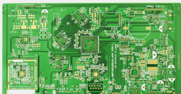
Evolution of Multilayer Circuit Boards
Multilayer printed circuit boards have revolutionized electronic products globally by offering advanced functionalities and complex wiring arrangements. The integration of components and wiring enhances the sophistication of modern circuit boards.
Enhanced Flexibility and Complexity
Advanced technology has enabled manufacturers to reduce the size of circuit boards significantly. Multilayer circuit boards, comprising a minimum of three layers of copper foil, provide enhanced options and choices for end-users.
Interconnectivity and Functionality
These boards consist of multiple layers resembling single or double-sided boards fused together by heat and protective insulation. The electrical connections between layers are established through blind holes and through holes, leading to the production of diverse circuit board sizes in the market.
The evolution of multilayer circuit boards has addressed previous issues such as crosstalk, capacitance, and noise, necessitating manufacturers to implement specific restrictions for control.
Design considerations play a pivotal role in achieving high performance levels, paving the way for the development of multi-layer circuit boards that cater to the increasing demand for compact electronic products.
The Advantages of Multi-Layer PCB
- Compact Size: Multi-layer circuit boards are smaller in size compared to single or double-layer boards, making them ideal for modern devices.
- Compact and Sturdy: These circuit boards are more compact and sturdy, commonly found in laptops, smartphones, and tablets, providing a lightweight structure.
- Reduced Weight: By eliminating the need for multiple connectors between layers, multi-layer PCBs reduce weight and enhance device mobility.
- High Quality: The meticulous planning and organization involved in creating multi-layer PCBs result in higher quality and reliability compared to single or double-layer boards.
- Improved Durability: Multi-layer circuit boards are highly durable, able to withstand weight, heat, and pressure due to multiple layers of insulation materials and adhesives.
- High Flexibility: Flexible construction technology allows for the creation of flexible multi-layer circuit boards suitable for bending and buckling applications, although flexibility decreases with more layers.
- Enhanced Power: Combining multiple layers into a single unit provides stronger connectivity, enabling higher speed and capacity even in small sizes.
- Single Connection Point: Multi-layer PCBs operate as a single unit with only one connection point, minimizing size and weight in electronic applications.