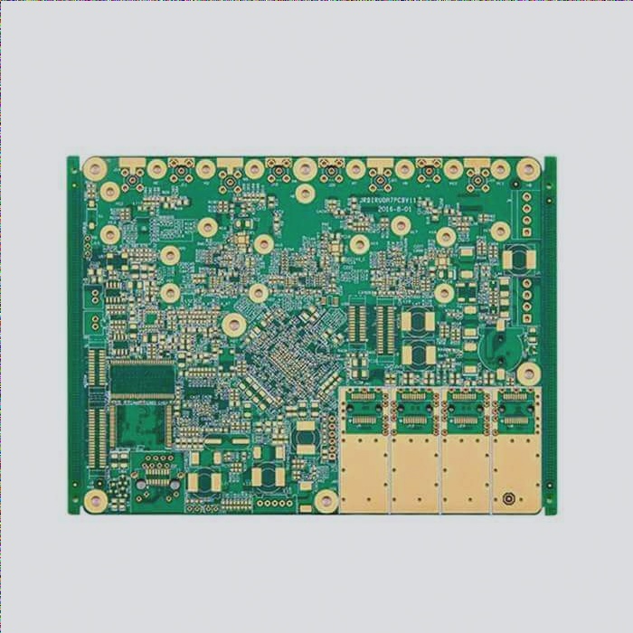
Design for Manufacturability (DFM) originates from product development and design, aiming to consider manufacturability and testability. It establishes a close relationship between design and manufacturing, striving towards the successful transition from design to manufacturing. This approach stands as the most effective method to ensure the quality of PCB design. In PCB design, DFM primarily encompasses device selection, PCB physical parameter selection, and attention to PCB design details.
1. **DFM Issues Impacting PCB Design**
The pads interfacing with devices on the PCB play a crucial role in determining whether the device can be soldered reliably. Compliance with IPC standards in pad design ensures proper soldering of components during manufacturing.
For SMD devices of sizes 0402, 0201, or smaller, achieving uniform pad connections is imperative. This prevents the tombstone effect, where components partially or fully detach from the board during reflow, leading to assembly failure.
2. **Avoidance of Vias in Pad**
The consensus in PCB design is to avoid Vias in Pad whenever possible, at all costs.
3. **Optimizing Placement of Through-Hole Devices (THTs)**
While many designers aim to minimize the use of through-hole devices or position them all on one side of the board, situations may demand their use. When combining through-hole and surface-mount components, proximity is key. Placing through-hole components on the top layer and surface-mount components on the bottom layer necessitates keeping all components as close together as feasible. However, this approach may impact single-sided wave soldering, prompting the utilization of more expensive soldering methods like selective soldering.
4. **Considerations for Copper Foil Distribution**
Creating a copper foil image on a single layer hinges on various factors. Uneven distribution of copper foil in specific areas can compromise the stability of individual traces. Hence, it is advisable to distribute copper foil evenly wherever possible.
5. **Optimal Pad and Spacing Sizes**
Many designers adhere to an empirical pad size of 50μm and a minimum spacing of 50μm between pads and traces. However, for the formation of solder bridges between two pads, the minimum size should be 75μm. These factors should inform the creation of component libraries and device placement on PCBs to prevent inadequate spacing that may fail to cover the area between pads adequately.


