Understanding High-Speed PCB Design
When delving into PCB designs like back drilling and teardrops, the mention of “high-speed applications” is common. But what exactly entails high-speed PCB design?
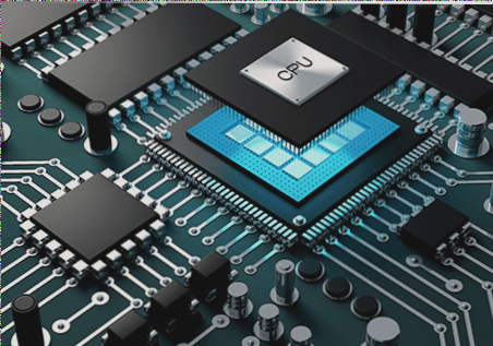
High-speed PCB design is tailored to support circuits, whether digital or analog, operating at frequencies typically exceeding 50 MHz. Industries like 5G networks, IoT devices, and high-performance computing heavily rely on high-speed design for swift and efficient data transmission.
Essential Aspects of High-Speed Design
- Signal Integrity: Signal integrity is crucial for seamless signal transmission in high-speed designs. Factors like signal loss, reflections, crosstalk, and noise can impact integrity. Techniques like robust grounding, controlled impedance traces, wider traces, and active components are employed to enhance signal integrity.
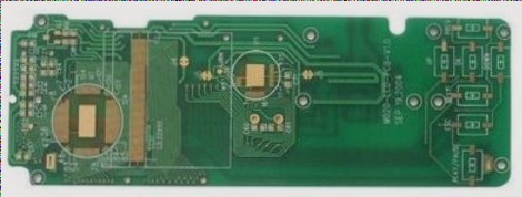
- PCB Substrate: High-speed circuits demand substrates with low Dielectric Constant for optimal electrical and thermal performance. Materials like Rogers 4350B and Rogers 4003C are preferred over standard FR-4 substrates due to their lower Dk values, reducing signal propagation delays and attenuation.
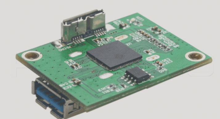
- Placement of Large ICs: Proper placement of large ICs like microprocessors and FPGAs is vital for system performance optimization. Placing them near connectors and minimizing interconnection lengths help improve signal integrity and reduce signal issues.
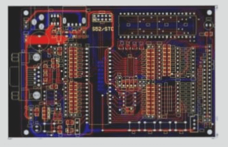
- Stack-up: Designing a proper PCB stack-up is critical in high-speed design. Utilizing reference planes, microstrip, and stripline traces aids in controlling impedance, reducing EMI, and enhancing signal integrity.
If you have inquiries regarding PCB or PCBA, don’t hesitate to reach out at info@wellcircuits.com.