In this article, we will explore Microstrip antennas, also known as printable antennas. These are a type of RF antenna that can be directly fabricated or printed onto a PCB (Printed Circuit Board).
The key topics we will cover include:
- Overview of Microstrip Antennas
- Structure of Microstrip Antennas
- Feeding Methods for Microstrip Antennas
Overview of Microstrip Antennas:
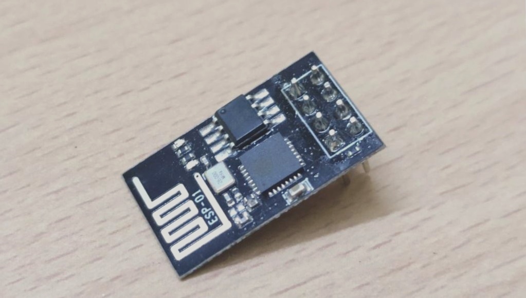
Microstrip antennas, also referred to as printed antennas, are a recent innovation that integrates the antenna directly with RF electronics on a PCB or silicon chip. This design allows for seamless integration of communication systems within compact devices.
Invented by Robert E. Munson, a distinguished antenna engineer at Ball Aerospace, the microstrip antenna revolutionized consumer electronics, particularly in wireless communication technologies such as Wi-Fi, Bluetooth, and other microwave-based systems. The invention made it possible to eliminate external antennas in devices like smartphones and laptops, as the antenna is now embedded directly on the PCB.
By integrating the antenna onto the PCB, the design remains sleek and compact. Imagine how bulky and outdated it would be if modern devices like smartphones or laptops still relied on retractable antennas, similar to older AM/FM radios!
Structure of a Microstrip Antenna:
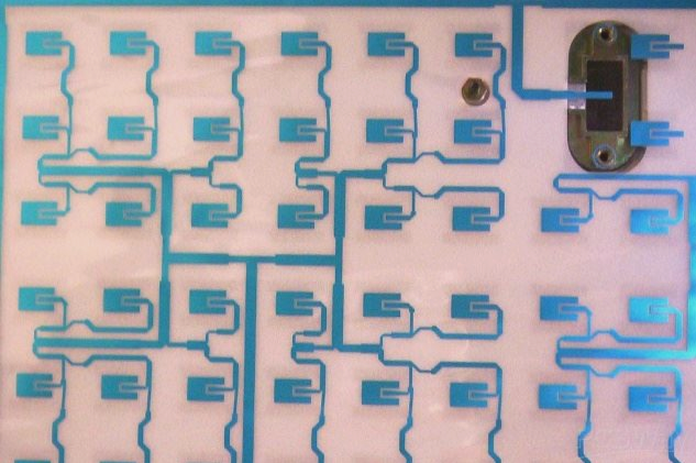
The image above shows a typical Microstrip antenna used in a satellite TV receiver. Below, we outline the basic components of a general Microstrip patch antenna.
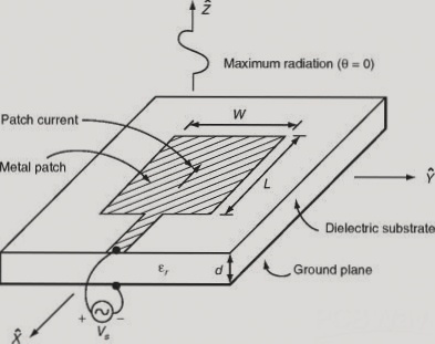
A Microstrip antenna typically consists of three main parts:
1) **Metal Patch**
2) **Dielectric Substrate**
3) **Ground Plane**
Let’s delve into the details of each component:
Metal Patch: The metal patch is typically made from copper or another conductive material and is designed with specific dimensions (length ‘L’ and width ‘W’) based on the operating frequency. The patch may be exposed or covered with a solder mask, depending on the design requirements.
Dielectric Substrate: The dielectric substrate is a non-conductive material that supports the metal patch. Its dielectric constant and thickness are critical factors that affect the antenna’s performance. The substrate material is usually the same as the PCB material, and its properties significantly influence the antenna’s efficiency and behavior.
Ground Plane: The ground plane is a continuous conductive layer placed on the opposite side of the dielectric substrate. It is typically larger than the metal patch and provides the necessary return path for the current, completing the antenna’s electrical circuit.
These three components—metal patch, dielectric substrate, and ground plane—work together to define the antenna’s operating frequency, bandwidth, and radiation pattern.
Feeding Methods for Microstrip Antennas:
Feeding methods refer to the techniques used to deliver the signal to a Microstrip antenna. There are several different feeding techniques, each with its own advantages and disadvantages. Below are the four most commonly used feeding methods:
1) **Line Feed Method**
2) **Probe Feed Method**
3) **Proximity Feed Method**
4) **Aperture Coupled Method**
Let’s examine each method in more detail:
Line Feed Method:
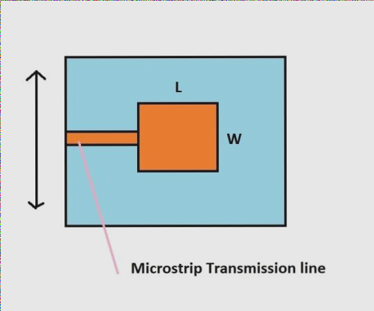
In the Line Feed method, a narrow conductive line connects to the metal patch, as shown in the image above. This transmission line is a Microstrip line that makes contact with both the RF circuit on the PCB and the patch itself.
Impedance matching is crucial in this method and is achieved by adjusting the position of the narrow transmission line. Proper impedance matching ensures maximum power transfer between the antenna and the signal source.
Advantages:
1) Easy to fabricate
2) Simple impedance matching
3) Cost-effective design
Disadvantages:
1) Limited bandwidth
2) Cross-polarization due to asymmetrical design
Probe Feed Method:
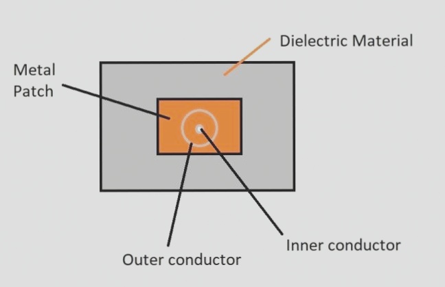
The Probe Feed method uses a coaxial cable, where the inner conductor is connected to the metal patch, and the outer conductor is connected to the ground plane. This setup offers another way of feeding the antenna signal.
Impedance matching in the probe feed method is achieved by adjusting the position of the inner and outer conductors relative to the patch.
Advantages:
1) Easy to fabricate
2) Simple impedance matching
3) Straightforward design
Disadvantages:
1) Limited bandwidth
2) Cross-polarization due to asymmetry
Proximity Feed Method:
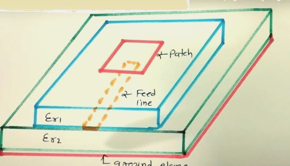
The Proximity Feed method involves two dielectric layers, with one attached to the metal patch and the other to the ground plane. The feed line is positioned between these two dielectric materials but does not make physical contact with either the patch or the ground plane.
Impedance matching is achieved by adjusting the length and width of the feed line.
Advantages:
1) Symmetrical design reduces cross-polarization
2) Higher bandwidth compared to other methods
3) Reduced spurious radiation
4) Easy to design
Disadvantages:
1) More difficult to fabricate due to multi-layer design
2) Higher cost compared to contact-based feeding methods
Aperture Coupled Method:
The Aperture Coupled method features a ground plane sandwiched between two dielectric layers. A patch is bonded to the top layer, while the feed line is attached to the bottom layer. This method is non-contact, as the feed line does not physically touch the patch or the ground plane.
Advantages:
1) Low cross-polarization
2) Moderate spurious radiation
3) Easy to design
Disadvantages:
1) Narrow bandwidth
2) Most complex and difficult to fabricate
Conclusion:
Microstrip antennas offer a cost-effective, efficient solution for integrating RF communication systems directly onto PCBs. These antennas are compact, easy to design, and capable of operating at microwave frequencies, making them ideal for modern wireless devices.
This post serves as an introduction to the subject, and we hope it inspires PCB designers and antenna engineers to further explore the potential of Microstrip antenna technology.
If you have any questions regarding PCBs or PCBA, please feel free to contact me at info@wellcircuits.com