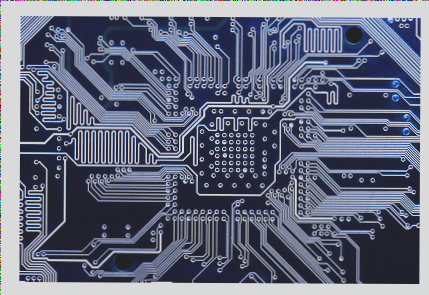
1. The PCB board consists of multiple layers of copper foil circuits, with connections between the various layers achieved through vias.

2. This is because modern PCB manufacturing uses drilled holes to establish electrical connections between different circuit layers, facilitating conductivity, which is why these connections are called vias.

3. To enable electrical conductivity, a layer of conductive material (typically copper) is plated onto the surface of the hole, allowing electrons to move between the copper foil layers. Without this plating, the surface of the drilled hole would be non-conductive.


1. **Through Hole (Plated Through Hole – PTH)**:

This is the most common type of via. Simply pick up the PCB and hold it up to the light; any hole through which light passes is a “through hole.” This is the simplest type of via, as it is made by drilling or laser cutting directly through the PCB, making the process relatively inexpensive. While through holes are cost-effective, they can sometimes occupy more space on the PCB. For example, imagine a six-story building where you buy the third and fourth floors and want to add a staircase connecting only these two floors. The staircase space on the fourth floor may end up occupying some of the area that was originally meant for the staircase between the first and sixth floors.

2. **Blind Hole (Blind Via Hole – BVH)**:

A blind via connects the outermost circuit layer of the PCB to an inner layer through a plated hole. Since the opposite side of the via is not visible, it is referred to as a “blind hole.” To maximize space utilization on the PCB, a “blind via” process is used. This process requires careful control of drilling depth (Z-axis) to ensure accuracy. The required holes are drilled in specific layers that need to be connected before the PCB is laminated. However, this requires precise positioning and alignment. Continuing with the building analogy: in a six-story building, the staircase only connects the first to the second floor, or the fifth to the sixth floor—these are considered blind vias.

3. **Buried Via (Buried Via Hole – BVH)**:

A buried via connects two inner circuit layers of the PCB but does not reach the outer layers. This type of via cannot be created after the PCB is laminated; it must be drilled in the individual circuit layers before they are bonded together. After the inner layers are partially bonded, they must undergo electroplating before the full lamination process can proceed. Compared to through holes and blind vias, buried vias take more time to produce, making them the most expensive option. This process is typically used for high-density interconnect (HDI) PCBs to maximize the available space on other layers. Referring again to the building example: in a six-story building, a buried via would be like having a staircase that only connects the third and fourth floors, with no access to the outer floors.

Leave a Comment

Contact

WellCircuits
More than PCB

Upload your GerberFile(7z,rar,zip)