The Top 10 PCB Assembly Design Mistakes to Avoid
When designing your PCB assembly, it’s crucial to steer clear of common mistakes that could lead to costly issues down the line. Here are the top 10 errors to watch out for:
- Early Engagement with EMS Partners: Involve your EMS partners from the get-go to prevent last-minute design flaws.
- Prototype and Preproduction Time: Allocate sufficient time for prototyping and preproduction to catch any unexpected glitches.
- Ideal Panel Size: Optimal panel size is key for smooth production line integration and component protection.
- Single-Sided SMT Components: Avoid unnecessary costs by carefully planning the placement of components on your PCB.
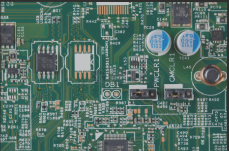
- Component Placement: Ensure components are correctly aligned and spaced on the PCB to prevent damage during assembly.
- Solder Paste Consideration: Balancing small and large components’ solder paste requirements is crucial for efficient assembly.
- Surface Treatment: Select surface treatments that suit your components to enhance longevity and reduce costs.
- Eliminating Unnecessary Test Points: Streamline your design by removing unnecessary test points to cut ongoing expenses.
- Soldering Concerns: Prevent short circuits by carefully planning component placement and soldering processes.
- Thorough Component Evaluation: To avoid design errors, thoroughly assess component compatibility and placement.
By steering clear of these common PCB assembly design mistakes, you can ensure a smoother production process and reduce costs in the long run.