**Multi-layer PCB Structure**
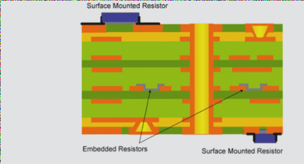
The multi-layer PCB consists of conductive materials, including the layers between the PCB and the additional signal layers. For example, a typical six-layer PCB includes two outer layers, two inner signal layers, one layer dedicated to power, and one for ground. This design enhances the suppression of electromagnetic interference (EMI) and provides more flexible routing options for both low-speed and high-speed signals. The two outer layers help with the routing of low-speed signals, while the inner layers are used for high-speed signal transmission.
**Six-layer PCB**
Proper stacking of a six-layer PCB can optimize its performance. With the integration of various types of radio frequency (RF) equipment, the design can effectively suppress EMI and accommodate multiple spacing components. Any design error can negatively impact the performance of the PCB. So, what should be considered during the design process to maximize the PCB’s potential?
First, before starting the design, it is essential to assess the required number of grounding, power, and signal planes for the PCB. Bonding layers are a critical component of any laminate, as they enhance shielding and reduce the need for external shielding cans.
For a compact, high-density circuit board, you may use four signal layers, along with a ground layer and a power layer. In high-density boards, both wireless and analog signals are often mixed. A stacking configuration of signal layer/ground/power/ground/signal/ground helps separate the inner and outer signal layers, creating distinct internal and external signal planes. This layered structure helps minimize EMI coupling within the inner signal layers. Such stacking designs are particularly suitable for RF applications, as the power and ground planes provide excellent decoupling.
**Dense PCB Circuit Board**

1. If you are designing a printed circuit board with multiple sensitive circuits, it is advisable to choose a stack-up like this: signal/power/2 signal/ground/signal. This configuration provides excellent protection for sensitive traces and is particularly well-suited for high-frequency analog or high-speed digital circuits. The sensitive signals are effectively isolated from low-speed signals on the outer layers, and the inner layers provide shielding, which also allows for the routing of signals with varying frequencies or switching speeds.
2. A PCB stack-up of ground/signal layer/power/ground/signal layer/ground can be strategically deployed near sources of strong radiation. This layout effectively mitigates electromagnetic interference and is ideal for circuit boards used in noisy environments.
3. Given that six-layer PCB designs have become a standard feature in advanced electronic circuits, and are widely adopted by electronic manufacturers, what exactly are the specific advantages they offer?
4. **Six-Layer PCB Design**
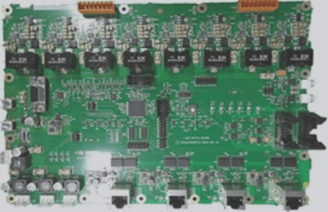
Due to their multi-layer construction, six-layer PCBs are relatively compact compared to other types of circuit boards, making them especially beneficial for miniature devices. The design of a six-layer PCB requires careful planning, which helps minimize design errors and ensures high-quality production. Nowadays, various testing and inspection methods are commonly used to verify the functionality of these circuit boards.
5. The compact nature of the printed circuit board is achieved through the use of lightweight components, which helps reduce the overall weight of the PCB. Unlike single-layer or double-layer boards, six-layer PCBs can connect components without the need for multiple PCB connectors.
6. The six-layer PCB consists of multiple insulating layers, created by bonding protective materials and different prepregs. This construction enhances the durability of the PCB.
7. The six-layer printed circuit board offers outstanding electrical performance and a compact design, ensuring high speed and large capacity for complex circuit applications.
If you have any PCB manufacturing needs, please do not hesitate to contact me.Contact me


