Understanding HDI Circuit Boards
An HDI circuit board, which stands for high-density interconnection PCB, utilizes advanced technologies to achieve high circuit distribution density. This is made possible through micro-blind and buried via technologies.
As the trend towards smaller and denser designs for portable products continues, PCB design has become more challenging. Most portable devices now utilize BGA packages with pitches smaller than 0.65mm, requiring the use of blind and buried via design processes.
Blind and Buried Vias in PCBs
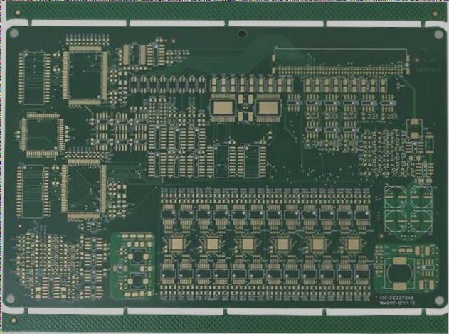
Blind and buried PCBs, also referred to as HDI boards, are commonly found in high-end applications like mobile phones and GPS navigation systems. Understanding the different types of PCB holes is crucial:
- Blind Vias: Connect inner PCB layers to outer layers without penetrating the entire board.
- Buried Vias: Connect traces between inner layers and are not visible from the PCB surface.
- Through Holes: Span the entire board and are visible from top to bottom layers.
The Evolution of PCB Design
With the evolution of PCB design, the focus is on accommodating more high-performance parts within limited PCB areas. As line density increases and packaging methods advance, the use of buried and blind vias becomes essential.
Aperture sizes have decreased significantly, from 1mm for DIP holes to less than 0.4mm for modern SMD components. To maximize surface area, buried and blind vias are utilized for internal connections within the high-density multi-layer board.
Manufacturing Blind Well Plates
There are three primary methods for manufacturing a blind well plate, each contributing to the intricate design of HDI circuit boards.