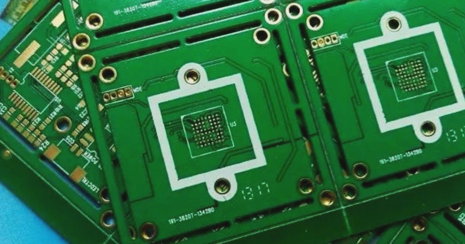
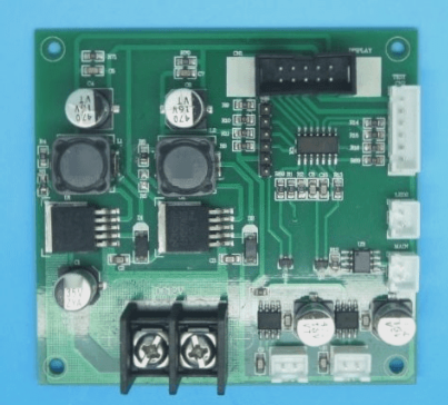
The so-called copper coating on a circuit board involves using the unused space on the board as the base surface, which is then filled with solid copper. These areas are commonly referred to as copper filling.
The importance of copper coating lies in its ability to reduce ground impedance and improve anti-interference capabilities. It also helps to decrease voltage drop and enhance power efficiency. Additionally, by connecting it with the ground wire, the loop area can be further minimized.
In order to ensure that PCB welding is done without deformation, most PCB manufacturers require designers to fill any open areas on the board with copper or a grid-like ground wire. If the copper is not handled properly, the potential drawbacks may outweigh the benefits. Therefore, it is crucial to consider whether the presence of copper on the board has a net positive impact or a net negative impact.
You all know that in the case of high frequency, the distributed capacitance of the wiring on the printed circuit board will have an effect. When the length is greater than 1/20 of the corresponding wavelength of the noise frequency, there will be an antenna effect, and the noise will be emitted outward through the wiring. If there is a poorly grounded copper coating on the PCB, the copper coating can actually become a tool for spreading noise.
Therefore, in high-frequency circuits, do not simply connect the ground wire to a certain point and assume it is the “ground”. The spacing between ground wires should be less than λ/20, with holes punched in the wiring and a well-grounded ground plane on the multilayer board. Properly treated copper coating not only increases the current, but also acts as a shield against interference.
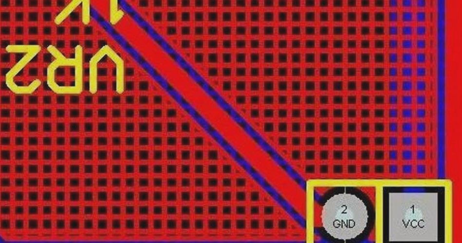
There are generally two basic methods of copper coating: large area copper coating and grid copper coating. It is often debated whether large area copper coating or grid copper coating is better, but there is no one-size-fits-all answer.
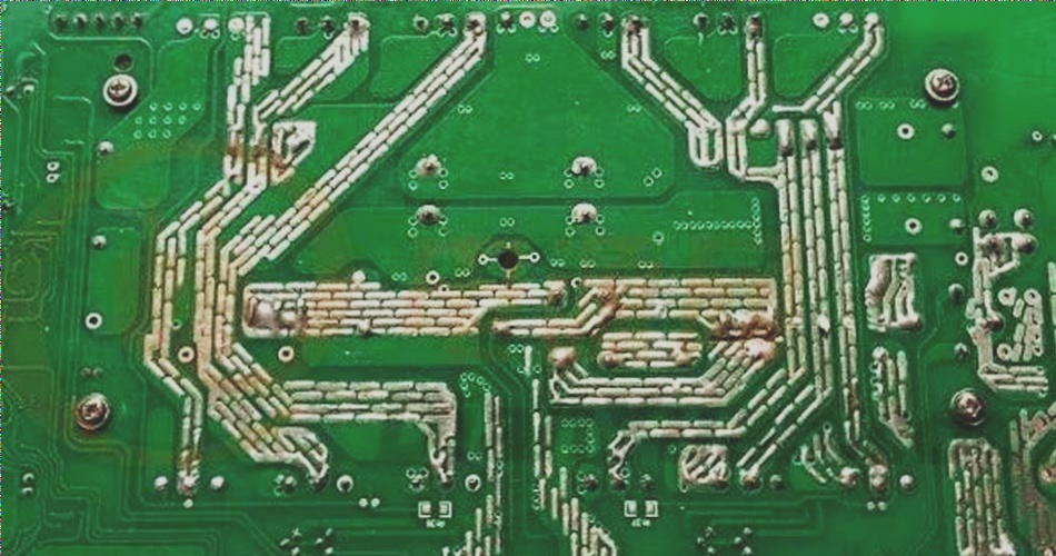
Why is this? Large-area copper coating has the benefit of increasing current and providing shielding, but if the copper coating is too large, it can cause issues during wave soldering, resulting in the board tilting or even foaming. Therefore, when using a large area of copper coating, it is common practice to open several slots to reduce the risk of foaming, as shown below:
The simple grid copper coating primarily functions as a shield, decreasing the current’s capacity. From a heat dissipation standpoint, the grid offers advantages by reducing the amount of copper exposed to heat, while also providing some electromagnetic shielding benefits. This is especially beneficial for circuits sensitive to touch.
It should be noted that PCB grids are composed of staggered traces, and it is important to consider the “electrical length” of the traces in relation to the working frequency of the circuit board. This can be determined by dividing the digital frequency corresponding to the working frequency, as detailed in relevant literature.
When the working frequency is not very high, the impact of the grid traces may not be significant. However, when the electrical length matches the working frequency, it can lead to malfunction and signal interference within the system.
It is advisable to select the appropriate grid design based on the circuit board requirements, rather than rigidly adhering to a specific approach. For high frequency circuits with strict interference requirements, a multi-purpose grid layout is recommended, while low frequency and high current circuits often benefit from a full copper pour design.