PCB Copy Boards: A Comprehensive Guide
When it comes to PCB copy boards, feelings of shame and anger may arise, whether you’ve copied someone else’s work or been a victim of copying. It’s crucial to evaluate the professionalism of your copying process and implement strategies to safeguard your designs from replication. One intriguing method worth exploring is the double-panel copying technique.
The Technical Process of PCB Copying
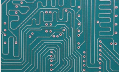
The technical process of PCB copying entails scanning the original circuit board, meticulously documenting component placements, and disassembling the board to generate a bill of materials (BOM) for component procurement. Additionally, you can utilize online tools to estimate PCB costs. The blank board is scanned, processed with copying software, and transformed into a PCB design file. This file is then forwarded to a fabrication facility for production. Following board creation, components are soldered, and rigorous testing and debugging procedures are conducted.
Specific Steps for PCB Copying
- Step 1: Document the model, parameters, and critical component positions of the PCB. Pay close attention to diode, transistor, and IC gap orientations. Capture two photos of these crucial components using a digital camera, as some components may not be immediately obvious on modern PCBs.
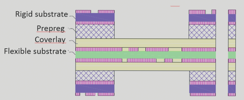
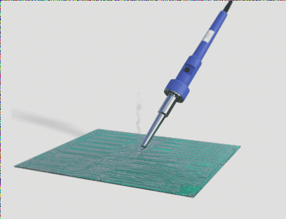
- Step 2: Disassemble multi-layer boards and prepare for copying by desoldering PAD holes and thoroughly cleaning the PCB with alcohol before scanning.
Feel free to reach out if you require further modifications or additional details!