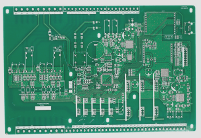
Just looking at the feasibility of a potential stupidly dense design on a 4 layer PCB
Ideally it would use a lot of blind vias between layers 1-2 and 3-4, but it seems this is an expensive process (compared to buried vias between 2-3).
I may be able to live with all the vias going all the way though if I could avoid having via pads on the layers that the don’t connect to, particularly the outer layers.
so for example I’d have a 0.15mm hole with 0.4mm pads on layers 1&2 only, or 3 & 4 only.
This is low-volume so needs to be compatible with a normal process
I don’t think I’ve seen a board like this, but can’t immediately think why it shouldn’t be possible – Anyone done this?


