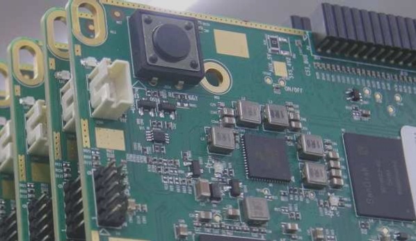
Designing Printed Circuit Boards with High-Speed FPGAs
As field programmable gate arrays (FPGAs) have advanced into programmable system-on-chips, the complexity of designing PCBs with these chips has increased. With circuit densities reaching millions of gates and data rates exceeding 6 Gbps, system developers face challenges in mechanical and electrical design efforts. To fully leverage the capabilities of FPGAs, careful PCB design is essential.
Key Considerations for High-Speed FPGA Design
- Reducing system noise through power distribution and filtering
- Properly terminating signal lines to minimize reflections
- Minimizing crosstalk between traces
- Addressing ground bounce and Vcc reduction effects
- Matching impedance on high-speed signal lines
Optimizing Pinout for Reduced Crosstalk
Optimizing pinout by placing signal pins close to ground pins helps minimize inductive coupling and reduces crosstalk effects on adjacent I/O pins within the package.
Enhancing Signal Integrity and Reducing Costs
Meticulous design of board materials, layer count, and layout is crucial to enhance signal integrity and reduce costs. Using EDA tools for optimal pinout and chip placement can lead to cost savings by reducing the number of required layers.
Managing High-Speed Signal Paths
Minimizing interruptions like vias and connectors on high-speed signal paths is essential to prevent signal edge rate reduction and reflections. Shortening via lengths and maintaining consistent via structures for differential signals are recommended.
Optimizing Clock Signal Integrity
For optimal clock signal integrity, keeping the signal on a single layer, utilizing a plane as reference, and proper termination are key. Utilizing on-chip termination resistors in FPGAs like the Stratix II GX family can enhance signal integrity and simplify board layout.

PCB Layout Best Practices for Minimizing Crosstalk
- Follow specific guidelines for microstrip and stripline routing to minimize crosstalk.
- In double-stripline layouts, confine wiring to two inner board layers with voltage reference surfaces on both sides.
- Use orthogonal wiring techniques in adjacent layer boards to maximize isolation between signal layers.
- Maintain consistent material thickness and normalized spacing between signal and adjacent reference planes to ensure requisite impedance.
- For microstrip or stripline routing, keep trace spacing at least three times the dielectric layer thickness between routing layers.
- Utilize simulation tools to predict behavior and optimize routing.
Reducing Common-Mode Noise in High-Speed Networks
- Prefer differential over single-ended topology to minimize common-mode noise effects.
- Attempt to match positive and negative pins within design limits.
- For single-ended signals, maintain adequate spacing (greater than three times the trace width) or use different board layers for routing.
- Simulation tools are essential for verifying spacing requirements and minimizing parallel lengths between signal terminations.
Addressing Simultaneous Switching Noise and Ground Bounce
- Simultaneous switching noise, clock frequencies, and I/O data rates can lead to ground bounce.
- Configure unused I/O pins as outputs driven low to mitigate ground bounce.
- Distribute simultaneous transition output pins evenly across the FPGA I/O section.
- Use low slew rates at FPGA outputs when high edge rates are unnecessary.
Optimizing Signal Integrity with Advanced Transceiver Capabilities
- Modern transceivers incorporate transmitter pre-emphasis and receiver equalization to counteract high-frequency channel distortions.
- These techniques extend the viability of standard FR-4 materials for higher data rates.
- Integrated programmable features in high-performance FPGAs support dynamic adjustment of pre-emphasis and equalization levels.
Minimizing Electromagnetic Interference (EMI) and Enhancing Design Reliability
- Efficient board design minimizes EMI by eliminating “hot” signals and grounding references.
- Surface mount components further reduce EMI.
- Utilize advanced tools such as JTAG with in-system programming and self-test capabilities for debugging and testing complex high-speed PCB designs.
Mastering High-Speed FPGA Design for Optimal Performance
- Designing with embedded high-speed FPGAs requires extensive practice and understanding of FPGA capabilities.
- Leverage pre-emphasis and equalization in transceivers to enhance design reliability and manufacturability.
- Comprehensive simulation and analysis preemptively identify issues in PCB prototypes, streamlining development and reducing project stress.