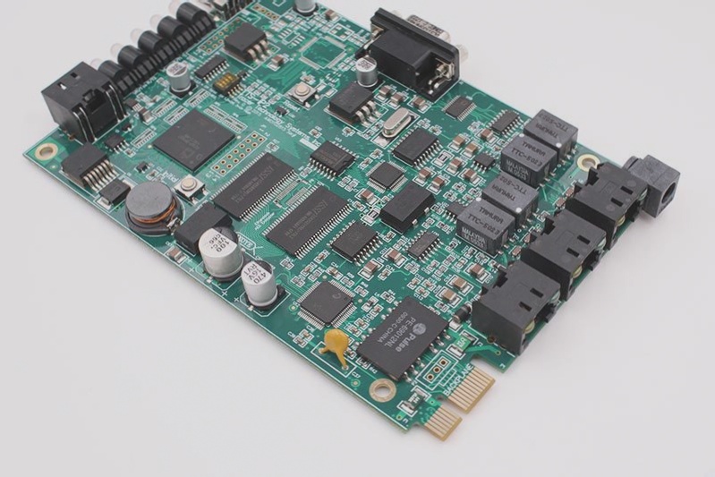
Physical Partition in RF Circuit Board Design
- Component Placement:
- Crucial for effective RF design.
- Position components along the RF path to minimize length.
- Separate RF input from RF output, high-power, and low-noise circuits.
- Implement efficient board stacking with the main ground on the second layer.
- RF Traces and Vias:
- Run RF traces on the surface layer.
- Reduce via size on the RF path to lower inductance and prevent RF energy leakage.
- Use linear circuits for RF zone isolation.
- RF and IF Traces Crossing:
- Cross RF and IF traces with a ground area in between to minimize interference.
- Proper RF routing is vital for optimal PCB performance.
- Component placement, especially in mobile phone PCB design, requires attention to detail.
- Special Considerations:
- Implement techniques to stop RF energy from passing through vias.
- Place LNA circuit and high-power amplifier on opposite sides, connected via a duplexer.
Metal Shield in RF Circuit Board Design
- Necessity and Drawbacks:
- Essential when achieving adequate separation is challenging.
- Drawbacks include high manufacturing costs, assembly challenges, and layout restrictions.
- Optimizing Metal Shield:
- Ensure integrity by routing digital signal lines to inner layers.
- Utilize the next layer as the ground layer.
- Allow RF signal lines to pass through shield gaps surrounded by a ground area.
- Drawbacks Mitigation:
- Despite limitations, metal shields effectively isolate critical circuits.

