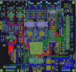
1. If you aim for longevity in the industry, prioritizing excellent quality reigns supreme, and the PCB sector is no exception. Robust PCB testing protocols are imperative for ensuring product integrity.
2. One of the most conventional testing methods involves inspectors utilizing magnifying glasses or calibrated microscopes to meticulously examine circuit boards for any irregularities. While this method incurs no test fixture costs, it suffers from drawbacks such as prolonged testing times, intermittent defect detection, and challenges in data collection.
3. However, as PCB production scales up, with reductions in wire spacing and component sizes, this method becomes limited to simple single-sided and complex double-sided multi-layer boards, often failing to detect underlying issues.
4. For enhanced accuracy in detecting PCB irregularities, conducting tests after each production process is advisable. This approach aids in assessing PCB yield and electrical performance, identifying manufacturing defects, and ensuring compliance with specifications. Test methods such as bed-of-needle testers and flying probe testers are commonly employed for this purpose.
5. Leveraging optical principles and integrating image analysis alongside other cutting-edge technologies facilitates the detection and resolution of production challenges.
6. Additionally, employing laser beam scanning during PCB fabrication enables comprehensive data collection, contributing to meticulous quality control throughout the manufacturing process.
Participate in test work promptly on the production line; engage in timely communication with the business department to understand customer needs, prepare for testing, and inform fellow PCB enthusiasts that the PCB testing cycle is short. Delay at the developer’s end can disrupt progress, leading to increased pressure on the PCB processing plant for production. Lack of communication with the business/ engineering departments or the production team results in inadequate understanding of product attributes, insufficient test data, prolonged testing, and reduced efficiency.
Establish a quality department communication group. Prior to initiating production orders, the quality department head should draft a detailed basic test requirements table for each PCB. A well-crafted, comprehensive test plan enhances the understanding of unique PCB requirements among online test staff, preventing aimless testing.
The quality manager should promptly review test documents, aiming for fewer test cases to uncover more bugs, thereby significantly enhancing test efficiency. This approach elevates the quality test acceptance standard and minimizes repeated testing of boards.
Conduct regular internal training sessions for testers to keep them updated on industry standards. Additionally, since testing entails extensive communication, employees need to engage with project managers, developers, product managers, colleagues in the business department, and customers. Proactive communication with the engineering, production, and customer departments helps grasp evolving customer requirements or changes, leading to smoother testing processes.
Sure, here’s a refined version of the text:
—
The test fixture used across industries remains consistent. In PCB manufacturing, the term “PCB test fixture” refers to a tool used to detect issues such as open circuits and short circuits on PCB boards. Almost all PCBs undergo testing, except for some simple single-sided panels which may be inspected visually. There are generally two methods for PCB testing: flying probe testing and test fixtures. Flying probe testing is suitable for small batch samples, but for larger batches, 98% of customers opt for using test fixtures.
Apart from being highly efficient, test fixtures incur a one-time cost, unlike flying probe tests which are charged per use. Furthermore, many PCB manufacturers offer the possibility of recovering the test fixture cost, often with refund thresholds set at specific production volumes such as 30,000 or 50,000 units, although these thresholds vary.
Materials required for manufacturing PCB test fixtures include acrylic sheets, positioning columns, thimbles, cards, and leads. The choice of materials for fixture production should be tailored to specific requirements to optimize production costs. Utilizing reusable base templates can further reduce costs and standardize fixture production, thereby enhancing fixture quality. Selecting appropriate test needles and related materials in test fixtures is crucial for ensuring both quality testing and cost-effectiveness.
当然,请把文章贴在这里,我会帮你逐行修改润色。