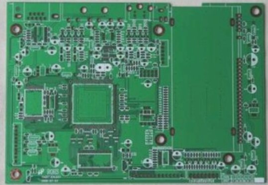
Understanding Printed Circuit Boards (PCBs)
- Printed Circuit Boards (PCBs) are essential components comprised of various elements and intricate manufacturing processes.
- PCBs can be single-layer, double-layer, or multi-layer, each with specific production techniques.
Components on a PCB
- Pad: Metal hole for soldering component pins
- Via: Metallic hole for inter-layer connections
- Mounting hole: Secures the PCB in place
- Wire: Copper film for electrical connections
- Connectors: Interconnect circuit boards
- Filling: Copper coating to reduce impedance
- Electrical boundary: Defines PCB size

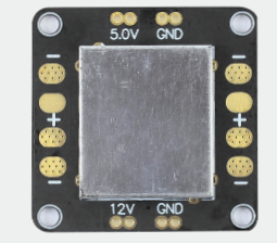
Types of PCB Structures
- Single-layer board: Copper on one side for wiring and soldering
- Double-layer board: Copper on both sides for component placement and soldering
- Multi-layer board: Contains multiple operational layers for various functions
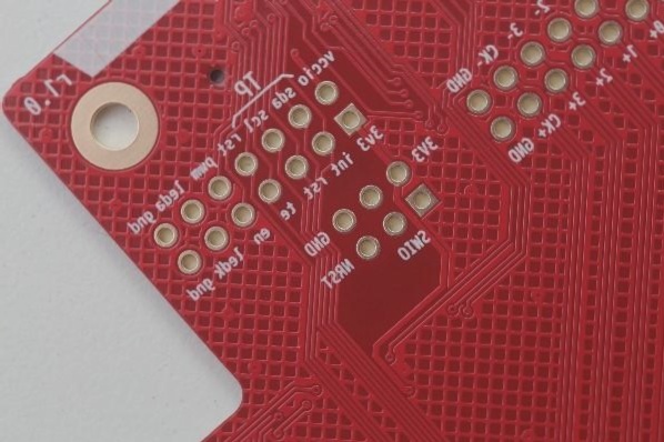
Working Layers on PCBs
- Signal layer: For component placement and wiring
- Protective layer: Enhances operational reliability
- Silk screen layer: Prints essential information on the PCB
- Internal layer: Functions as a signal wiring layer
- Other layers: Include Drill Guide for drilling hole positions
Explore the intricate world of PCBs and their diverse applications to enhance your understanding of electronic components.