For PCB layout engineers, it is important to move beyond being seen as mere “wire pullers” and cultivate a deeper understanding of the fundamental principles behind the layout process. Broadening one’s knowledge in PCB design is crucial to achieving high-performance circuits. A key aspect of this is understanding the reasoning behind the design choices, rather than simply following guidelines based on experience. In this article, I will share some important principles derived from years of experience in PCB design, which can help PCB layout engineers make more informed and effective decisions.
### 1. Component Placement: Prioritize Function and Modularity
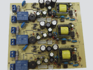
The first and most important step in any PCB design is the placement of components. A well-organized layout ensures that the function of the circuit is clear and that the components are easily identifiable by anyone with a basic understanding of the circuit’s purpose. This modular approach allows for easy troubleshooting, modification, and maintenance of the board. A good rule of thumb is to group components according to their functional blocks. For example, power components (such as voltage regulators) should be placed close to power inputs, while signal processing components should be grouped together. This modular layout minimizes signal interference and simplifies routing.
### 2. Signal Integrity: Maintain Proper Trace Design
Once components are placed, the next step is to route the traces. Signal integrity is one of the most critical aspects of PCB layout, especially for high-speed designs. To ensure signal integrity, several factors must be considered:
– **Trace Length and Width**: The length of the signal traces should be kept as short as possible to reduce parasitic inductance and capacitance. In high-speed circuits, longer traces can lead to signal degradation and reflection issues. Similarly, trace width must be chosen carefully to maintain the correct impedance, especially for high-frequency signals.
– **Signal Parallelism**: When routing multiple signals, it is important to avoid parallel traces that are too close to each other. This can lead to crosstalk between signals, where one signal interferes with another, compromising signal quality. Keeping traces apart and ensuring adequate spacing between them helps reduce interference.
– **Trace Impedance Matching**: For high-speed digital or RF signals, maintaining a consistent impedance along the trace is crucial to prevent signal reflections. This is typically achieved by adjusting the trace width and the distance between the trace and the reference plane (ground or power).
### 3. Grounding and Power Distribution: Ensure Stability and Minimize Noise
A well-designed ground plane is essential for maintaining the overall stability of the circuit. The ground plane should be as continuous and unbroken as possible to minimize noise and provide a solid return path for current. For power distribution, the layout should ensure that each component receives a stable and sufficient supply of power. This can be achieved by using wide power traces or planes to reduce voltage drops and minimize noise.
– **Decoupling Capacitors**: Place decoupling capacitors as close as possible to power pins of ICs to filter high-frequency noise. This helps ensure that the components receive clean and stable power, reducing the likelihood of power-related performance issues.
– **Avoiding Ground Loops**: Ground loops can introduce noise into the system, leading to signal interference and stability problems. To avoid ground loops, ensure that all ground connections converge to a single point, known as a “star grounding” configuration.
### 4. Thermal Management: Prevent Overheating
Overheating is a common issue in PCB design, particularly when components dissipate significant amounts of power. Proper thermal management is crucial to ensure the longevity and reliability of the circuit. Key strategies include:
– **Thermal Vias**: Use thermal vias to transfer heat from the component to the back side of the PCB or to a dedicated heat sink. This helps distribute heat evenly and prevents hotspots.
– **Component Placement**: Place heat-sensitive components away from heat-generating components, such as power transistors or voltage regulators. Additionally, ensure that there is sufficient space for airflow or heat dissipation.
– **Copper Area for Heat Dissipation**: Increase the copper area around high-power components to improve heat dissipation. Using larger copper areas or incorporating copper pours in power areas helps lower the temperature of critical components.
### 5. Design for Manufacturability (DFM): Consider Production Constraints
Lastly, it is important to consider manufacturability during the layout process. A well-designed PCB should not only meet performance requirements but also be cost-effective and manufacturable. DFM principles help identify potential production issues early in the design process, such as:
– **Minimizing Layer Count**: Reducing the number of layers in the PCB design helps lower manufacturing costs and simplifies the fabrication process. This can often be achieved through careful component placement and efficient routing.
– **Clearance and Tolerances**: Ensure that there is adequate clearance between traces and pads, and that tolerances are within acceptable limits for the manufacturing process. This avoids issues such as short circuits or unreliable connections.
### Conclusion
In summary, PCB layout is a complex and critical aspect of hardware design that goes far beyond simple trace routing. It requires a deep understanding of signal integrity, power distribution, grounding, thermal management, and manufacturability. By applying these principles and continuously expanding one’s knowledge, PCB layout engineers can move beyond being “wire pullers” and contribute to the creation of high-performance, reliable circuits. Continuous learning and thoughtful application of best practices will not only improve the quality of the PCB design but also the overall performance of the hardware system.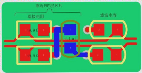
### PCB Design Steps and Best Practices
#### 1. Initial PCB Design and Layout
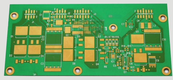
The first step in PCB design is generating the initial PCB file based on the schematic diagram. This involves completing the pre-layout phase, which includes determining the relative PCB layout area. The next task is to define the structure within this area, ensuring it aligns with the given constraints. The overall structure design should be based on these guidelines, and any specific constraints, such as size limitations or component positioning, should be clearly defined at this stage.
#### 2. Board Edge, Positioning, and Forbidden Areas
Once the structural constraints are established, begin drawing the board edges, including positioning openings and defining areas where component placement is restricted (i.e., forbidden areas). Afterward, place the connectors in appropriate locations, taking into consideration ease of access and signal integrity.
#### 3. Component Placement Principles
In typical PCB designs, the placement of components follows specific principles to ensure efficient performance:
– **Microcontroller (MCU)**: Place the main control unit (MCU) at the center of the board to minimize signal path lengths.
– **Interfaces**: Position interface circuits near the corresponding physical interface (e.g., network port, USB, VGA). Additionally, ensure that most interfaces are protected by ESD (electrostatic discharge) protection and filtered to reduce noise.
– **Power Modules**: The main power module (e.g., 5V system power) is typically placed near the power inlet. Secondary power modules (e.g., 2.5V power for specific modules) can be placed in denser areas, provided they share the same power network.
– **Circuit Organization**: When designing internal circuits that do not connect to external connectors, organize them into distinct regions such as high-speed and low-speed areas, analog and digital areas, or sensitive and noisy regions. This helps minimize interference.
#### 4. High-Level Circuit Layout
When designing individual circuit modules, follow the direction of current flow in your layout. Ensuring a well-structured, logical flow is key to optimizing signal integrity and minimizing noise. The overall circuit layout should aim to simplify routing and minimize interference. Any additional design insights or corrections are welcome.
### Wiring Guidelines for PCB Design
#### 1. Signal Connectivity and Effectiveness
The primary goal during PCB wiring is to ensure all networks are connected correctly. While basic connectivity is easy to achieve, effectiveness refers to the quality of the signal transmission. In digital circuits, this means ensuring noise immunity, while in analog circuits, it is essential to minimize signal loss.
#### 2. Layer Design and Signal Routing
Before starting the wiring, it’s critical to plan the PCB stack-up design, which defines the signal layers and power planes. The optimal wiring layer should be a continuous ground plane, which helps in routing critical signals such as DDR, differential signals, and analog signals. Non-critical signals (e.g., I2C, UART, SPI) can be routed on other layers.
For high-speed signals, issues like reflection, crosstalk, and electromagnetic compatibility (EMC) should be carefully considered. Impedance matching is crucial, with common values being 50 ohms for single-ended lines and 100 ohms for differential pairs. The design should ensure that impedance remains consistent and continuous.
#### 3. Power Supply Design and Return Paths
Ensure that the power supply network has sufficient load capacity, with thick and short return paths for current. From an EMC perspective, minimizing the return loop area helps to reduce radiation and noise. The return paths should be as direct and compact as possible to prevent the formation of unwanted radiative loops.
### Grounding Strategies in PCB Design
#### 1. Importance of Grounding
Grounding is a fundamental aspect of PCB design, as the ground plane serves as the reference for all other signals. A poorly designed ground plane can lead to signal instability and degraded performance. Therefore, ensuring a solid, continuous ground is essential for reliable operation.
#### 2. Types of Ground
Ground can generally be divided into two types:
– **Chassis Ground**: This is connected to the metal enclosure of the product.
– **System Ground**: This serves as the reference plane for the entire circuit system, ensuring a stable voltage reference for all components.
#### 3. Ground Plane Separation
It is best practice to separate the chassis ground from the system ground. These two grounds should be connected at a single point, typically through a magnetic bead or a high-voltage capacitor. This method prevents noise from the chassis affecting the system ground.
#### 4. Dividing System Ground
In a complex PCB design, the system ground can be further divided into digital ground, analog ground, and power ground regions. However, if the PCB layout is well-organized with distinct areas for digital, analog, and power circuits, a single, continuous ground plane may be sufficient. This simplifies routing and ensures that all currents return directly to their respective ground planes.
By adhering to these principles, you can design a PCB that minimizes noise, reduces signal integrity issues, and improves overall performance. If you have additional suggestions or improvements, feel free to contribute.