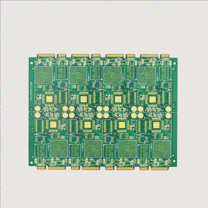
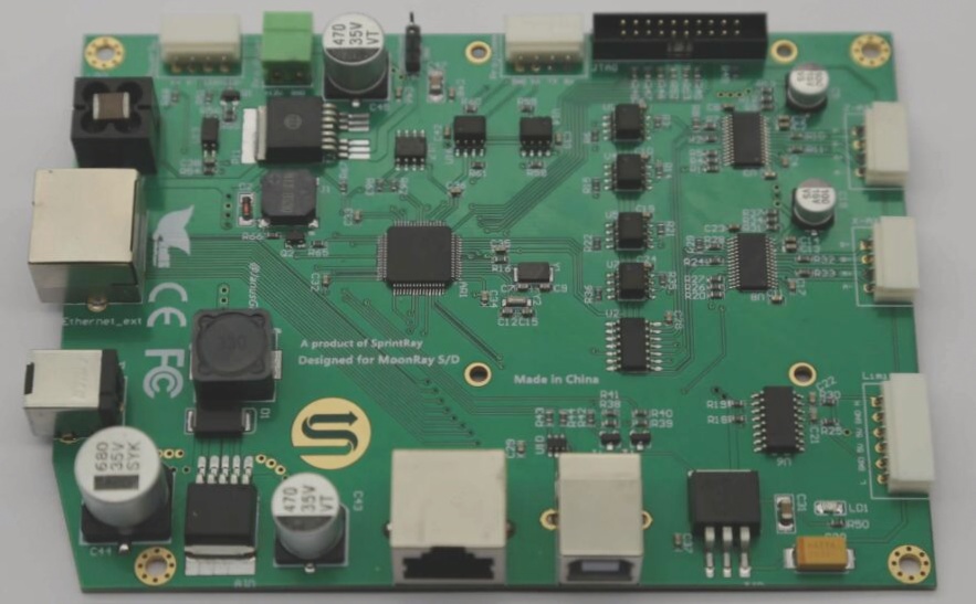
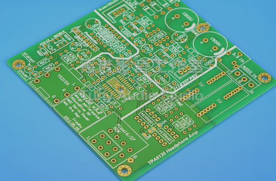
Wiring is one of the most delicate and intricate skills in the PCB board design process. Even engineers with over a decade of experience often find wiring challenging, having encountered numerous problems and potential issues with various layouts. The potential negative consequences can make it difficult to know how to proceed. However, there are experts who excel in this area. They combine rational knowledge with a touch of personal creativity, resulting in aesthetically pleasing and highly functional wire layouts. Here are some useful tips and essentials for effective wiring:

1. To start, let’s provide a basic overview. PCB boards can be categorized into single-layer, double-layer, and multi-layer configurations. Single-layer boards are largely obsolete now. Double-layer boards are commonly used in audio systems, particularly for power amplifiers, and are often sufficient for their intended applications. From the perspective of via holes, they can be classified as through holes, blind holes, or buried holes. A through hole extends from the top layer to the bottom layer; a blind hole connects either the top or bottom layer to an intermediate layer without continuing through to the other side. The advantage of blind holes is that their position remains clear for routing on other layers. A buried via, on the other hand, is contained entirely within the internal layers and is not visible on the surface.

2. Before relying on automatic routing, manually route the lines with higher requirements. Ensure that the edges of the input and output ends are neither adjacent nor parallel to avoid reflection interference. When necessary, add a ground wire for isolation, and ensure that the wirings on adjacent layers are perpendicular to each other to minimize parasitic coupling. The effectiveness of automatic routing largely depends on a good layout. Pre-set routing rules, such as the number of wire bends, vias, and steps, to guide the process. Typically, exploratory wiring is done first, connecting short lines quickly, followed by optimizing the global wiring path through iterative routing to achieve the best overall effect.

3. For layout, a key principle is to separate digital and analog circuits as much as possible. Additionally, avoid placing low-speed signals close to high-speed ones. A fundamental principle is to keep digital and analog grounds separate. Digital grounding involves large current fluctuations due to switching, which can interfere with analog signals. Therefore, it is crucial not to mix digital and analog grounds. A recommended layout strategy is illustrated in the image below.

1. Precautions for Wiring Between Power Supply and Ground Wire

1) **A decoupling capacitor** should be added between the power supply and the ground wire. The power supply must be connected to the chip pins through this decoupling capacitor. The following figure illustrates several incorrect connection methods and one correct method; please refer to it. Have you made such mistakes? Generally, decoupling capacitors serve two functions: providing instantaneous large currents to the chip and filtering out power supply noise. This helps minimize the noise that can affect the chip.

2) **Widen the power and ground wires** as much as possible. The ground wire should be wider than the power wire, in the order: ground wire > power wire > signal wire.

3) **Utilize a large copper area as the ground wire.** Connect unused areas of the printed board to the ground to serve as additional ground wire, or design a multi-layer board with separate layers for the power supply and ground.

2. Handling Mixed Digital and Analog Circuits

Nowadays, many PCBs are a mix of digital and analog circuits. It’s crucial to address potential mutual interference, particularly noise on the ground wire. Due to the high frequency of digital circuits and the sensitivity of analog circuits, high-frequency signal lines should be kept away from sensitive analog components. On the PCB, there should be only one ground node to avoid external sensitivity issues. Internally, the grounds of digital and analog circuits should be separated but joined at a single point on the PCB, such as at a plug. Ensure that there is only one common ground point, as determined by the system design.

3. Handling Line Corners

Changes in wire thickness at corners can cause reflections. For corner thickness changes, right angles should be avoided; 45-degree angles are better, and rounded corners are ideal. However, rounded corners are more complex to design, so typically, a 45-degree angle is sufficient for most signals. Only highly sensitive lines may require rounded corners.

4. Checking Design Rules After Wiring

Regardless of the task, a final check is essential. Just as you review exam answers, reviewing the PCB design ensures a high-quality product. Check the following aspects:

1) Verify that the distances between wires, wires and component pads, wires and through holes, component pads and through holes, and through holes are reasonable and meet production requirements.

2) Ensure that the widths of the power and ground lines are appropriate, that they are tightly coupled (low wave impedance), and if there are any areas where the ground line can be widened.

3) Confirm that key signal lines have been properly managed, such as keeping their lengths short, adding protection lines, and clearly separating input and output lines.

4) Check that the analog and digital circuits have separate ground wires.

5) Ensure that added graphics on the PCB do not cause signal short circuits.

6) Modify any unsatisfactory line shapes.

7) Verify that the PCB has proper process lines, that the solder mask meets production requirements, that the solder mask size is appropriate, and that text labels are correctly placed on the device pads to avoid affecting electrical quality.

8) Ensure that the edge of the power ground layer in multi-layer boards is properly reduced to prevent short circuits, such as copper foil exposure outside the board.

In summary, these skills and methods are based on experience and are valuable when designing PCBs. Besides proficient use of drawing tools and software, solid theoretical knowledge and practical experience are crucial. Attention to detail during the design process is essential, as small mistakes can render the final product unusable. It is better to spend extra time carefully checking details during the drawing process than to deal with problems later, which can be more time-consuming.

Leave a Comment

Contact

WellCircuits
More than PCB

Upload your GerberFile(7z,rar,zip)