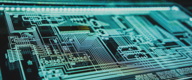
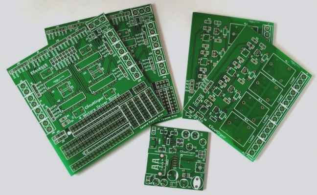
There are specific processes and precautions for the design and production of circuit boards. The copper coating of circuit boards is a critical step in PCB design with significant technical complexity. To effectively manage this phase, experienced engineers have summarized the following key practices:
1. At high frequencies, the distributed capacitance of the PCB wiring will play a role. When the length exceeds 1/20 of the corresponding wavelength of the noise frequency, an antenna effect may occur, leading to noise emission through the wiring. Poorly grounded copper cladding can act as a conduit for noise transmission. Thus, in high-frequency circuits, simply connecting a ground wire does not suffice. Instead, ensure a pitch less than λ/20 and create “good ground” by connecting the wiring to the ground plane of the multilayer board. Proper copper coating can enhance current flow and provide effective shielding against interference.
2. For copper coating to be effective, several issues must be considered:
– If the PCB has multiple grounds (e.g., SGND, AGND, GND), use the main “ground” as a reference and independently pour copper for digital and analog grounds. Ensure that the copper pour is separated as needed. Before pouring copper, first thicken the corresponding power connections (e.g., 5.0V, 3.3V) to create various multi-deformation structures.
– For single-point connections between different grounds, use 0-ohm resistors, magnetic beads, or inductors.
– Copper pour should be applied near the crystal oscillator. Since the crystal oscillator is a high-frequency emission source, surround it with copper and ground it separately.

4. If the island (dead zone) problem seems significant, defining a ground via and adding it should not be costly.
5. At the beginning of the wiring, treat the ground wire with equal importance. Ensure proper routing of the ground wire; relying on adding via holes after copper pour to fix connections is ineffective and leads to poor results.
6. Avoid sharp corners (<=180 degrees) on the board. From an electromagnetic perspective, sharp corners can act as antennas, potentially affecting nearby components. It’s better to use rounded edges.
7. Avoid pouring copper in the open areas of the middle layer of a multi-layer PCB. It is challenging to ensure that this copper provides a reliable ground.
8. Ensure that metal components within the equipment, such as radiators and reinforcement strips, are properly grounded.
9. The heat dissipation metal block of a three-terminal regulator and the ground isolation strip near the crystal oscillator must be well grounded. Proper grounding of PCB copper is crucial as it reduces signal return area and minimizes electromagnetic interference.
1. At high frequencies, the distributed capacitance of the PCB wiring will play a role. When the length exceeds 1/20 of the corresponding wavelength of the noise frequency, an antenna effect may occur, leading to noise emission through the wiring. Poorly grounded copper cladding can act as a conduit for noise transmission. Thus, in high-frequency circuits, simply connecting a ground wire does not suffice. Instead, ensure a pitch less than λ/20 and create “good ground” by connecting the wiring to the ground plane of the multilayer board. Proper copper coating can enhance current flow and provide effective shielding against interference.
2. For copper coating to be effective, several issues must be considered:
– If the PCB has multiple grounds (e.g., SGND, AGND, GND), use the main “ground” as a reference and independently pour copper for digital and analog grounds. Ensure that the copper pour is separated as needed. Before pouring copper, first thicken the corresponding power connections (e.g., 5.0V, 3.3V) to create various multi-deformation structures.
– For single-point connections between different grounds, use 0-ohm resistors, magnetic beads, or inductors.
– Copper pour should be applied near the crystal oscillator. Since the crystal oscillator is a high-frequency emission source, surround it with copper and ground it separately.

4. If the island (dead zone) problem seems significant, defining a ground via and adding it should not be costly.
5. At the beginning of the wiring, treat the ground wire with equal importance. Ensure proper routing of the ground wire; relying on adding via holes after copper pour to fix connections is ineffective and leads to poor results.
6. Avoid sharp corners (<=180 degrees) on the board. From an electromagnetic perspective, sharp corners can act as antennas, potentially affecting nearby components. It’s better to use rounded edges.
7. Avoid pouring copper in the open areas of the middle layer of a multi-layer PCB. It is challenging to ensure that this copper provides a reliable ground.
8. Ensure that metal components within the equipment, such as radiators and reinforcement strips, are properly grounded.
9. The heat dissipation metal block of a three-terminal regulator and the ground isolation strip near the crystal oscillator must be well grounded. Proper grounding of PCB copper is crucial as it reduces signal return area and minimizes electromagnetic interference.


