Key Considerations for Effective PCB Design
- The purpose of PCB design should always be clear and well-defined. For critical signal lines, precise control over the trace length and grounding loop design is essential.
- In contrast, for low-speed or less important signal lines, wiring can be given a lower priority in terms of routing and layout considerations.
Important Areas to Focus on:
- Power distribution
- Memory clock lines
- Control lines and data line length requirements
- High-speed differential pair routing, etc.
Example: Memory Chip Design for Project A
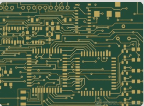
In Project A, a 1G DDR memory chip is used, and its wiring plays a pivotal role in the overall design. Special care must be taken in the topological arrangement of the control, address, and data lines. Additional considerations include the control of length differences between data and clock lines, as well as the precise routing of high-speed signals.
To ensure optimal signal integrity and performance, it’s necessary to refer to the chip’s datasheet and the operating frequency to establish specific wiring rules.
Conversion of Requirements into Design Constraints
Once critical design requirements are established, they can be translated into comprehensive wiring constraints for the PCB layout. By defining these constraints clearly, designers can use automated routing tools in CAD software to ensure adherence to specified rules, aligning with current trends in high-speed PCB design.

Debugging Process
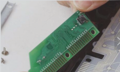
When preparing to debug a PCB, start with a thorough visual inspection to check for visible issues like short circuits, pin tinning problems, or incorrect component placements. Use a multimeter to measure resistance between power supplies and ground to detect potential short circuits. Approach debugging with patience, systematically analyzing and eliminating possible causes.
Summary and Reflection
Success in a project goes beyond technical execution. Factors like meeting deadlines, maintaining product quality, and effective team collaboration are crucial. Good teamwork, open communication, meticulous planning, and resource management are essential for project success.
A competent hardware engineer also acts as a project manager, understanding design requirements, communicating with relevant parties, and selecting the right components. Collaboration with CAD engineers, preparing BOM lists, sourcing materials, and coordinating with manufacturers are all part of the process.
Collaboration and Ongoing Support in Hardware Engineering
Effective collaboration among hardware engineers, software engineers, and test engineers is essential for successful debugging processes. Hardware engineers play a critical role in providing ongoing support post-deployment to address any potential issues that may arise.
Key Skills for Hardware Designers
- Excellent communication skills
- Ability to work well under pressure
- Capacity to manage multiple tasks simultaneously
Attention to detail and diligence are crucial attributes for hardware designers, as even minor oversights can result in significant financial repercussions.
Importance of Thorough Inspection
For instance, a simple error in the manufacturing files, such as incorrectly connecting power and ground layers, can lead to severe consequences. Neglecting inspection before production can result in unnoticed issues like short circuits, causing substantial losses once components are soldered.
Continuous Learning and Responsible Testing
Emphasizing thorough inspection, responsible testing practices, and a commitment to continuous learning are vital for the advancement and success of hardware engineers in their careers.