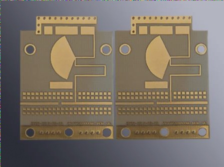
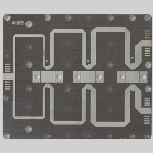
1 The preferred process route has been determined and all devices have been placed on the PCB board.
2 The coordinate origin is the intersection point between the lower left extension line of the board frame and the lower extension line, or the lower left solder pad of the lower left corner socket.
3 Maintain device spacing to avoid short circuits or overheating caused by being too close.
4 Choose the appropriate wiring direction, try to straighten the wiring as much as possible, and reduce bends with too small angles.
5 Ensure that the wiring width is sufficient to meet current and impedance requirements, and leave appropriate margin.
6 Properly arrange the routing of power and ground wires to reduce noise interference.
7 For multi-layer boards, it is necessary to allocate the signal layer, power layer, and ground layer reasonably.
8 Reserve sufficient board edge spacing and hole spacing to meet manufacturing and assembly requirements.
9 Reasonably arrange the hole positions to avoid overlapping with wiring or other components.
10 Pay attention to the layout of thermal sensitive components, stay away from heat sources, and have a good heat dissipation path.

3. The PCB’s actual size, positioning device location, etc. must align with the process structure element diagram. Additionally, the device layout in areas with limited device height requirements should meet the structure element diagram’s specifications.
4. The placement of dial switches, reset devices, indicator lights, etc. should be appropriate, ensuring that the handlebar does not interfere with surrounding devices.
5. The outer frame of the board should have a smooth radius of 197mil. Alternatively, it can be designed according to the structural dimension drawing.
6. For ordinary boards, there should be a 200mil process edge. The left and right sides of the backplate should have a process edge larger than 400mil, while the upper and lower sides should have a process edge larger than 680mil. The device placement must not conflict with the window opening position.
7. All additional holes that need to be added (such as ICT positioning hole 125mil, handle strip hole, elliptical hole, and fiber support hole) must be correctly set.
8. The device pin spacing, device orientation, device spacing, device library, etc. that are processed by wave soldering should consider the requirements of wave soldering processing.
9. The spacing between device layouts should meet the assembly requirements: surface mount devices should be greater than 20mil, ICs should be greater than 80mil, and BGAs should be greater than 200mil.
10. The crimping element should have a surface distance of more than 120 mils above it. Additionally, there should be no devices in the through area of the crimping element on the soldering surface.
11. There should be no short devices between tall devices. SMD devices and short and small plug-in devices should not be placed within 5mm between devices with a height greater than 10mm.
12. Polarity devices should be marked with polar silkscreen. The X and Y directions of the same type of polarized plug-in components should be the same.
13. All devices must be clearly marked, and there should be no unclear markings like P*, REF, etc.
14. A surface containing SMD devices should have 3 positioning cursors placed in an “L” shape. The distance between the center of the positioning cursor and the edge of the board should be greater than 240mil.
15. If panel processing is needed, the layout should be designed to be easy to make up, facilitating PCB processing and assembly.
16. The gaps (special-shaped edges) on the board’s edge should be filled using milling groove and stamp hole methods. The stamp hole should be a non-metallized hole, typically with a diameter of 40 mils and located 16 mils from the edge.
17. Test points for debugging should be added in the schematic diagram, and their positions in the layout should be appropriate. Additionally, the layout should consider thermal design requirements.
18. The heating element and exposed devices in the shell should not be placed close to wires and thermal elements. Other devices should also be appropriately kept away.
19. When placing the radiator, the layout must consider convection problems and avoid high device interference in the radiator’s projection area. The range should be marked on the mounting surface with silk screen.
20. The layout should consider reasonable and smooth cooling channels.
21. Electrolytic capacitors should be properly separated from high-heat devices.
22. The heat dissipation of high-power devices and devices under the gusset should be taken into account.
Signal Integrity Requirements for Layout
23. Origin matching should be close to the transmitting device, while termination matching should be close to the receiving device.
24. Decoupling capacitors should be placed close to related devices.
25. Crystals, crystal oscillators, and clock driver chips should be placed close to related devices.
26. High-speed and low-speed, digital and analog signals should be divided into modules.
27. The bus topology should be determined based on analysis, simulation results, or existing experience to ensure system requirements are met.
28. If modifications are made to the board design, signal integrity problems observed during testing should be simulated and solutions provided.
29. The layout of the synchronous clock bus system should meet timing requirements.
EMC Requirements
30. Inductive devices prone to magnetic field coupling such as inductors, relays, and transformers should not be placed close to each other. When multiple inductor coils are present, they should be oriented vertically to avoid coupling.
31. To avoid electromagnetic interference between devices on the soldering surface of the veneer and adjacent veneers, sensitive devices and devices with strong radiation should not be placed on the soldering surface of the veneer.
32. Interface devices should be placed close to the board’s edge, and appropriate EMC protection measures (such as shielding cases or hollowing out power supply ground) should be implemented to improve EMC capability.
33. Protection circuits should be placed near interface circuits, following the principle of protection first and filtering later.
34. Devices with high transmit power or particularly sensitive devices (such as crystal oscillators, crystals, etc.) should be located at least 500 mils away from the shield and shield shell.
35. A 0.1uF capacitor should be placed near the reset line of the reset switch to keep the reset device and signal away from other strong devices and signals.
Layer Setup and Power Ground Splitting Requirements
36. Clear rules for vertical routing must be defined when two signal layers are directly adjacent.
37. The main power supply layer should be adjacent to its corresponding ground layer as much as possible. The power supply layer should abide by the 20H rule.
38. Each routing layer should have a complete reference plane.
39. In stacked multi-layer boards, the core material (CORE) should be symmetrical to prevent uneven density distribution of copper skin and asymmetric thickness of the medium that could cause warping.
40. The thickness of the board should not exceed 4.5mm. For boards thicker than 2.5mm (backplanes greater than 3mm), technicians should confirm that there are no issues with PCB processing, assembly, and equipment. The thickness of PC card boards is typically 1.6mm.
41. If the aspect ratio of vias exceeds 10:1, it should be confirmed by the PCB manufacturer.
42. The power supply and ground of the optical module should be separated from other power supplies and grounds to reduce interference.
43. The power supply and ground processing of key devices should meet the requirements.
44. If impedance control is required, the layer setting parameters should meet the requirements.
Power Module Requirements
45. The layout of the power supply part should ensure smooth and non-crossing input and output lines.
46. When a single board supplies power to the pinch board, the corresponding filter circuit should be placed near the power outlet of the single board and the power inlet of the pinch board.
Other Requirements
47. The layout should consider overall wiring smoothness and reasonable main data flow.
48. Based on the layout results, adjust the pin assignments of devices such as resistor exclusion, FPGA, EPLD, bus driver, etc. to facilitate wiring.
49. The layout should allow for increased space for dense traces to avoid situations where routing becomes impossible.
50. If special materials, special devices (such as 0.5mmBGA, etc.), and special processes are used, the delivery period and machinability should be fully considered and confirmed by PCB manufacturers and craftsmen.
51. The pin-to-pin correspondence of the gusset connector should be confirmed to prevent the direction and orientation of the connector from being reversed.
52. If there are ICT test requirements, the feasibility of adding ICT test points should be considered during layout to avoid difficulties in adding test points during the wiring phase.
53. When including high-speed optical modules, the layout should prioritize the optical port transceiver circuit.
54. After the layout is completed, a 1:1 assembly drawing should be provided to enable the project team to check if the device package selection is correct against the physical components.
55. The inner plane should be indented at the window opening, and an appropriate prohibited wiring area should be set on the PCB board.


