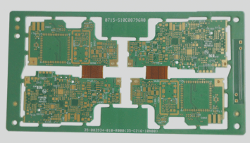
The Significance of PCB Layout in High-Speed Circuit Design
Efficient manufacturing of Printed Circuit Boards (PCBs) for high-speed circuits is crucial for the success of the final product. However, the importance of PCB layout design is often underestimated during the development process. Early and meticulous planning, along with adherence to key design principles, can greatly enhance both functionality and manufacturability.
Latest Insights:
- Recent studies suggest that incorporating artificial intelligence algorithms in PCB layout design can optimize signal routing and minimize interference, leading to improved circuit performance.
- Advanced simulation tools now allow designers to predict and mitigate signal integrity issues in high-speed circuits before fabrication, reducing the need for costly redesigns.
- Emerging trends in PCB manufacturing, such as additive manufacturing techniques and flexible substrates, are revolutionizing the design possibilities for high-speed circuits.
Key Considerations for Successful PCB Design in High-Speed Circuits
- Schematic Documentation
Detailed schematics are crucial for a high-quality PCB layout, providing a clear representation of the circuit flow and aiding in early issue identification. - Signal Integrity and Trace Routing
Proper trace routing techniques, including differential pair routing and controlled impedance traces, are essential for maintaining signal integrity in high-speed designs. - Component Placement and Grounding
Effective component placement and grounding strategies are vital for minimizing noise and interference in high-speed circuits. - Thermal Management
Implementing thermal management techniques, such as thermal vias and copper pours, is critical for heat dissipation in high-speed circuits. - Design for Manufacturability (DFM)
Compliance with DFM guidelines ensures that high-speed PCB designs are not only functional but also manufacturable at scale, reducing production risks and delays.
The Importance of Layout in High-Speed PCB Design
When it comes to high-speed circuit design, the layout of a PCB plays a crucial role in determining the overall performance and manufacturability of the final product. By incorporating key design principles early on, such as clear schematic documentation, precise trace routing, strategic component placement, proper grounding, efficient thermal management, and adherence to DFM considerations, designers can avoid costly redesigns and ensure the PCB functions as intended during production.
Latest Insights in High-Speed PCB Design
- Collaboration for Success: Collaboration between designers and engineers is essential to meet design standards and functional requirements, ultimately leading to a PCB that performs optimally.
- Strategic Component Placement: Careful placement of components is vital to optimize performance and prevent interference between circuits.
- Power Supply Optimization: Implementing effective power supply bypassing techniques and utilizing decoupling capacitors can reduce noise levels for stable operation.
- Managing Parasitic Effects: Identifying and controlling parasitic capacitance and inductance early on can help maintain circuit stability.
- Signal Integrity Solutions: Proper wiring techniques and shielding methods can minimize signal interference and improve overall performance.
- Material Selection Impact: Choosing materials with suitable dielectric constants is crucial for signal transmission speed and noise reduction.
- Trace Design Optimization: Trace width, thickness, and substrate material properties directly influence signal quality and noise isolation.
Key Considerations for Successful High-Speed PCB Design
Key Principles for Successful High-Speed PCB Design
- Adherence to established best practices and guidelines is crucial for designing high-speed PCBs that function as intended.
- Documenting all design constraints and updating them regularly can help minimize troubleshooting and rework.
- Developing a clear hierarchy of design considerations allows PCB engineers to focus on critical elements early in the process.
Successful high-speed PCB design involves collaboration, careful component placement, noise management, and understanding material and trace characteristics. By following these best practices, designers can create reliable and efficient PCBs.
If you need assistance with PCB or PCBA, feel free to contact us at info@wellcircuits.com.


