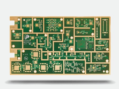
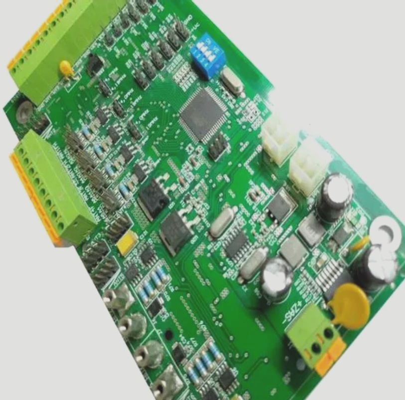
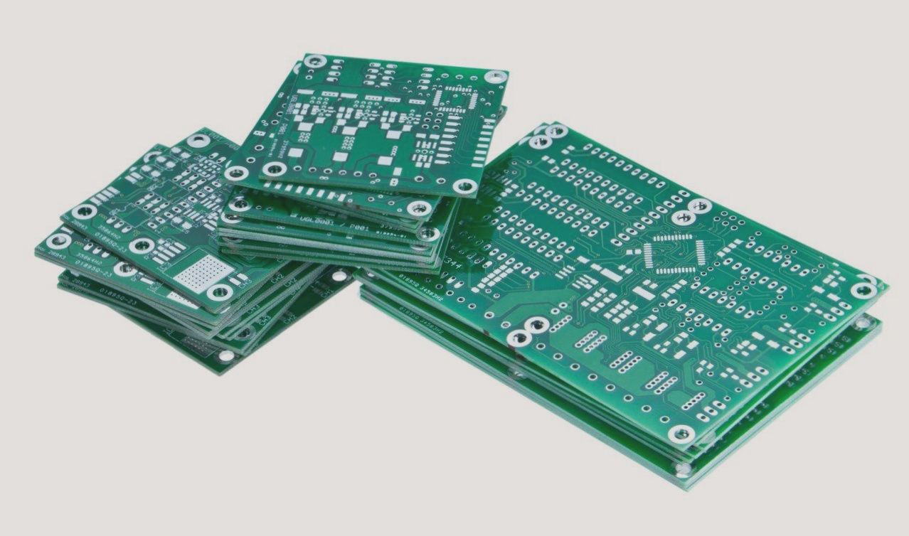
With the rapid development of the PCB industry, an increasing number of engineers and technicians are entering the field of PCB board design and manufacturing. However, many PCB design engineers (layout staff) have not been directly involved in the production and manufacturing processes of PCB boards, as the industry spans numerous disciplines. Consequently, during the design phase, there is often a strong focus on electrical performance and product functionality. Yet, problems arise downstream when PCB processing facilities receive orders. These issues stem from designs that overlook challenges in production, leading to extended processing times or potential product flaws.
To address such issues that hinder efficient processing and production, this analysis will examine seven critical aspects: cutting, drilling, wiring, solder mask, characters, surface treatment, and forming.

1. The choice of PCB material primarily hinges on plate and copper thickness. For plates thicker than 0.8mm, standard options include 1.0, 1.2, 1.6, 2.0, and 3.2mm, while thinner plates of less than 0.8mm utilize 0.4 and 0.6mm, typically for inner layers of multilayer boards. When selecting outer layer thickness, factors such as copper plating, solder mask thickness, surface treatment (e.g., tin spraying, gold plating), and character/carbon oil thickness must be considered. Tin plating typically ranges from 0.075-0.15mm thicker than required. For instance, a design specifying 2.0mm thickness would typically use a 2.0mm sheet, but considering sheet tolerance and processing, the final thickness might range from 2.1-2.3mm. If design specifications mandate a thickness no greater than 2.0mm, an unconventional 1.9mm board material would be required, necessitating special ordering from manufacturers, leading to extended delivery cycles. During inner layer fabrication, prepreg (PP) thickness and structural configuration influence post-lamination thickness adjustment, offering flexibility in core board selection. Even a standard 2.0mm thickness can alternatively be 1.0mm, provided lamination ensures final product thickness requirements are met. Additionally, plate thickness tolerance impacts product assembly tolerance. PCB designers should account for material, lamination, and outer layer thickening tolerances. Common sheet tolerances are: (0.8-1.0)±0.1, (1.2-1.6)±0.13, 2.0±0.18, and 3.0±0.23. Lamination tolerances within ±(0.05-0.1) vary based on layer and thickness differences in millimeters. For boards featuring edge connectors, board thickness and tolerance requirements are adjusted to match connector specifications.
2. Drilling considerations focus on hole size tolerance, especially with larger pre-drilled holes. Issues arise concerning hole proximity to board edges, non-metallized holes, and positioning hole design. Current mechanical drilling tips typically measure 0.2mm, necessitating enlarged design apertures due to copper thickness on hole walls and protective layer thickness. Tin spray plates may require a 0.15mm increase, while gold plating may require 0.1mm. The critical concern here is ensuring that enlarged hole diameters maintain sufficient distance from circuit traces and copper layers, and adequate solder ring coverage on designed circuit pads. Aperture tolerance for domestic drilling rigs is usually ±0.05mm, combined with coating thickness tolerance, resulting in ±0.075mm for metallized holes and ±0.05mm for non-metallized holes. Overlooked issues include isolation distance from drilled holes to inner layer copper or wires in multilayer boards, impacted by drilling positioning tolerance and graphic expansion/deformation during lamination. Design must guarantee a minimum distance of 0.15mm for 4-layer boards and 0.2mm for 6 or 8-layer boards to facilitate production. Non-metallized holes employ methods such as dry film sealing or colloidal plugging, ensuring no copper skin within 0.2mm of the hole perimeter. Design of positioning holes is critical for secure board fixture during circuit board processing, testing, or shape punching. Holes larger than 1.5mm must be strategically positioned, preferably forming a triangular distribution on circuit board corners.
3. Circuit fabrication involves circuit etching considerations due to lateral corrosion effects, requiring pre-thickened circuits. Standard compensations for copper thickness in tin spray and gold immersion processes are typically 0.025mm for HOZ copper, and 0.05-0.075mm for 1OZ copper, while line width/spacing production capacity is conventionally 0.075/0.075mm. Special attention is given to line width compensation during production, particularly for gold-plated boards where the gold layer’s presence after etching eliminates the need for compensation. However, side etching may reduce copper skin width under the gold layer, risking solderability issues with excessive copper thickness or etching. Lines with impedance requirements impose stricter line width/spacing conditions.
4. Solder mask production complexities primarily involve treatment of vias. Apart from their conductive function, vias often serve as test points or component plug-in holes. Standard vias require solder mask coverage to prevent soldering during assembly. Vias used for testing or plug-in purposes necessitate open windows to avoid trapping tin beads. For BGA packaging convenience, vias are treated with plugged oil. Apertures larger than 0.6mm complicate oil plugging, thus half-open window designs are adopted for tin-spray plates, ensuring a 0.065mm larger aperture than the via diameter. Character processing involves careful placement of pads and related marks. As component layouts become denser, pads must be positioned away from character prints, ensuring a minimum 0.15mm distance. In cases where component frames or symbols cannot be distributed on the circuit board, consider printing only the character frame to resolve design constraints. Essential marks include supplier identification, UL certification, flame retardant ratings, anti-static markings, production timelines, and customer-specific identifiers, each designated with clear meaning and specific placement.
5. Surface coating (plating) layers impact PCB design significantly. Widely used treatments include OSP, immersion gold, and tin spraying, each offering distinct advantages in cost, weldability, wear resistance, oxidation resistance, and production process compatibility. OSP boasts low cost and good conductivity but suffers poor oxidation resistance, necessitating post-formation cleaning. Nickel-gold electroplating provides excellent oxidation and wear resistance but demands current assistance during gold plating to avoid excessive copper etching under the gold layer. Electroless nickel gold plating (immersion gold) ensures good oxidation resistance and flat coating, suitable for SMT boards. Spray tin plating offers good oxidation resistance but poorer flatness compared to immersion gold. Recent surface treatment advancements, driven by the EU’s ROHS directive, include lead-free options such as pure tin and tin-silver-copper, replacing traditional lead-tin spraying processes.
6. Shape production complexities are essential considerations during PCB design. Electric milling intervals should align with milling cutter diameters (typically 1.6, 1.2, 1.0, 0.8mm). V-CUT connections require specific edge-to-copper sheet distances to ensure proper operation. Maximizing material utilization involves careful selection of standard sheet sizes (e.g., 930X1245, 1040X1245, 1090X1245). Mismanagement can lead to material wastage during delivery.


