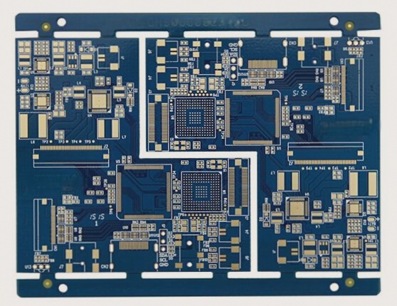
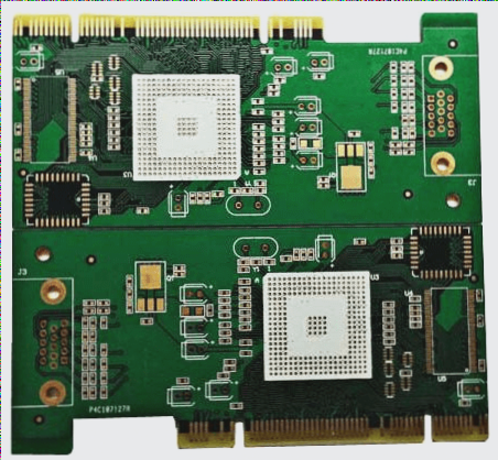
Introduction:
Electronic devices are essential in our daily routines and professional environments. The design of a printed circuit board (PCB) is pivotal in determining the functionality and effectiveness of these devices. Factors like grounding design, electromagnetic compatibility, PCB size, and heat dissipation are crucial for ensuring reliable performance during production and usage.
Latest Trends in PCB Design:
The world of PCB design is constantly evolving to meet the demands of modern technology. Some of the latest trends in PCB design include:
- 1. Miniaturization:
With the rise of wearable technology and IoT devices, there is a growing need for smaller and more compact PCB designs to fit into smaller gadgets without compromising performance.
- 2. High-Speed PCBs:
As data transfer speeds increase, there is a push towards high-speed PCBs that can handle the demands of technologies like 5G and high-definition video streaming.
- 3. Flexible and Rigid-Flex PCBs:
Flexible and rigid-flex PCBs are gaining popularity for applications requiring bendable or curved designs, such as wearables, medical devices, and aerospace systems.
Key Aspects of PCB Design:
- 1. Grounding Design Considerations:
The grounding system in a PCB consists of analog ground, digital ground, enclosure ground, and system ground. A well-designed grounding system is crucial for shielding interference and ensuring the proper functioning of electronic equipment.
- 2. Choosing the Right Grounding Method:
Grounding methods like multi-point and single-point grounding play a vital role in minimizing electromagnetic interference based on operational frequencies and circuit conditions.
- For frequencies above 10 MHz, multi-point grounding is recommended to reduce electromagnetic interference effects.
- For frequencies below 1 MHz, single-point grounding suffices to prevent electromagnetic circulation.
- For frequencies between 1 MHz and 10 MHz, the choice depends on circuit wavelength and ground trace length, with multi-point grounding preferred for shorter wavelengths.
- 3. Circuit Segregation for Different Properties:
To minimize interference between analog and digital circuits on a PCB, they should be physically separated. Implementing separate grounding systems for these circuits can significantly reduce electromagnetic interference.
- 4. Sizing of Grounding Wires:
Grounding wires should be wide and thick to prevent ground potential instability caused by current fluctuations. Using wires with a cross-sectional area of at least 3 mm² enhances noise resistance and improves overall device performance.
If you have any inquiries about PCB or PCBA design, please don’t hesitate to reach out to us at info@wellcircuits.com.


