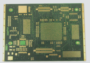
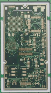
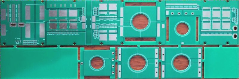
1. Regardless of the software chosen, there exists a standard procedure for PCB design. Adhering to this order can save both time and effort, so I will present it in accordance with the production process. (Due to Protel’s interface being similar to Windows, its operating habits are also comparable. With robust simulation capabilities and a large user base, this software will serve as our reference.)
2. Schematic design is the initial stage. It is common to see beginners jumping straight to PCB layout to avoid extra steps, but this approach can lead to more problems than it solves. While proficient users may bypass this step for simple boards, beginners should adhere to the process to foster good habits and prevent errors in complex circuits.
3. As an electronic engineer, designing a circuit requires significant effort. However, no matter how well-conceived the schematic design is, poor PCB layout can severely degrade performance or even result in malfunction. From my experience, I’ve outlined several critical considerations in PCB design, hoping to provide valuable insights.

1. When creating a schematic diagram, it’s crucial to ensure that all files are interconnected in the hierarchical design, which significantly impacts future tasks. Due to software variations, some programs might show components as connected when they aren’t (in terms of electrical performance). Without the appropriate testing tools, discovering issues post-assembly can be too late. Hence, the importance of a systematic approach cannot be overstated, and I encourage everyone to heed this advice.
2. The PCB schematic diagram stems from the designed project; as long as the electrical connections are accurate, there’s little else to discuss. Here, we will focus on challenges encountered in the board-making process.
3. Establishing a physical frame
The closed physical frame serves as a fundamental platform for future component layout and wiring, providing necessary constraints for automatic layout. Without it, components derived from the schematic may become disoriented. Accuracy is essential here, as future installation issues could arise if neglected. Additionally, using arcs at the corners is advisable; this not only prevents sharp edges from injuring workers but also mitigates stress effects. I once had a product where the PCB broke during transit, but switching to arcs resolved the issue.
4. Component and network introduction
Drawing components and networks within the frame should be straightforward, yet errors frequently occur. It’s essential to address these issues systematically according to the prompts; otherwise, troubleshooting can become laborious. Common problems include unavailable component packages, network issues, and unused components or pins, all of which can be swiftly resolved through comparison.
5. Component layout
The arrangement and wiring of components significantly influence the product’s lifespan, stability, and electromagnetic compatibility, warranting careful attention. The following principles should generally be observed:
5.1 Placement order
Begin by positioning structural components, such as power sockets, indicator lights, switches, and connectors. Once these are placed, use the software’s LOCK function to prevent accidental movement. Following this, arrange specialized and larger components like heating elements, transformers, and ICs, and finally, position smaller devices.
5.2 PCB layout considerations for heat dissipation
The layout must prioritize heat dissipation, particularly for high-power circuits. Heating elements, such as power tubes and transformers, should be placed near the edges to facilitate cooling. Avoid clustering components in one area, and keep high capacitors spaced apart to prevent premature electrolyte aging.
2. Schematic design is the initial stage. It is common to see beginners jumping straight to PCB layout to avoid extra steps, but this approach can lead to more problems than it solves. While proficient users may bypass this step for simple boards, beginners should adhere to the process to foster good habits and prevent errors in complex circuits.
3. As an electronic engineer, designing a circuit requires significant effort. However, no matter how well-conceived the schematic design is, poor PCB layout can severely degrade performance or even result in malfunction. From my experience, I’ve outlined several critical considerations in PCB design, hoping to provide valuable insights.

1. When creating a schematic diagram, it’s crucial to ensure that all files are interconnected in the hierarchical design, which significantly impacts future tasks. Due to software variations, some programs might show components as connected when they aren’t (in terms of electrical performance). Without the appropriate testing tools, discovering issues post-assembly can be too late. Hence, the importance of a systematic approach cannot be overstated, and I encourage everyone to heed this advice.
2. The PCB schematic diagram stems from the designed project; as long as the electrical connections are accurate, there’s little else to discuss. Here, we will focus on challenges encountered in the board-making process.
3. Establishing a physical frame
The closed physical frame serves as a fundamental platform for future component layout and wiring, providing necessary constraints for automatic layout. Without it, components derived from the schematic may become disoriented. Accuracy is essential here, as future installation issues could arise if neglected. Additionally, using arcs at the corners is advisable; this not only prevents sharp edges from injuring workers but also mitigates stress effects. I once had a product where the PCB broke during transit, but switching to arcs resolved the issue.
4. Component and network introduction
Drawing components and networks within the frame should be straightforward, yet errors frequently occur. It’s essential to address these issues systematically according to the prompts; otherwise, troubleshooting can become laborious. Common problems include unavailable component packages, network issues, and unused components or pins, all of which can be swiftly resolved through comparison.
5. Component layout
The arrangement and wiring of components significantly influence the product’s lifespan, stability, and electromagnetic compatibility, warranting careful attention. The following principles should generally be observed:
5.1 Placement order
Begin by positioning structural components, such as power sockets, indicator lights, switches, and connectors. Once these are placed, use the software’s LOCK function to prevent accidental movement. Following this, arrange specialized and larger components like heating elements, transformers, and ICs, and finally, position smaller devices.
5.2 PCB layout considerations for heat dissipation
The layout must prioritize heat dissipation, particularly for high-power circuits. Heating elements, such as power tubes and transformers, should be placed near the edges to facilitate cooling. Avoid clustering components in one area, and keep high capacitors spaced apart to prevent premature electrolyte aging.


