Improving PCB Design for Efficient Assembly
Enhancing PCB Manufacturability for Smoother Assembly Processes
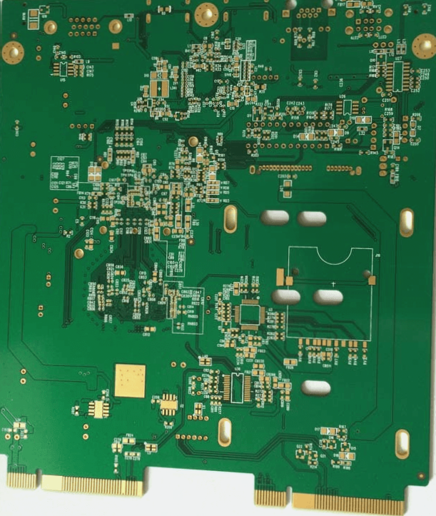
When dealing with PCBs of varying shapes and sizes, challenges may arise during the assembly phase. A common solution involves combining smaller PCBs to create a more manageable larger assembly, as depicted in Figure 5.
For PCBs with a single-side size below 150mm, the boarding method is typically employed. By merging two, three, or four smaller boards, a larger PCB assembly within the ideal range for automated processing (widths between 150mm and 250mm, lengths between 250mm and 350mm) can be achieved. This approach ensures efficient automated assembly.
Key Aspects of PCB Assembly Manufacturability
- Choice of Assembly Method: Selecting the right assembly method is crucial for cost-effective production. Options include through-hole technology (THT), surface-mount technology (SMT), and hybrid methods, each with specific requirements for component placement and board size.
- Component Layout: Proper component arrangement on the PCB greatly impacts assembly efficiency. Strategic placement reduces handling steps, minimizes errors, and speeds up assembly.
- Design for Testability: Incorporating test points and accessible pads in the design facilitates post-assembly testing, aiding in early issue detection and minimizing rework.
- Design for Reflow and Wave Soldering: Layout considerations for reflow and wave soldering processes are essential to ensure proper soldering and prevent thermal interference.
- Minimizing Component Variability: Standardizing component types and reducing variability in sizes, shapes, and lead configurations simplifies assembly, lowers costs, and eases inventory management.
Manufacturability plays a vital role in the efficiency of PCB assembly processes. By addressing these key considerations during the design phase, designers can optimize assembly outcomes and enhance overall production effectiveness.
For more information on PCB fabrication and assembly, visit Well Circuits.
Explore PCB assembly services for your next project.
Optimizing PCB Assembly for Efficiency and Quality
Key Considerations and Best Practices
-
Selection of an Appropriate Assembly Method
Choosing the right assembly method for a printed circuit board (PCB) is crucial, considering assembly density and wiring complexity. Aligning the method with company capabilities and standard processes is essential to avoid challenges.
-
Component Layout for Efficiency and Cost
Proper component layout enhances production efficiency and cost-effectiveness. Components should be arranged consistently, supporting faster patch speeds and heat dissipation. Prioritize compatibility with soldering processes for optimal results.
-
Standardizing Component Orientation
Standardizing component orientation improves assembly efficiency and simplifies troubleshooting. Aligning terminals and notches uniformly can increase insertion speeds and ease error detection.
-
Managing High-Density Assemblies
In high-density designs, challenges arise with components like tantalum capacitors and fine-pitch devices. Utilize double-sided solder paste printing and structured component placement to enhance efficiency and quality.
-
Consistency Between Components and Silk-Screen Symbols
Ensuring consistency between components and silk-screen symbols aids in assembly accuracy and reduces errors. Clear guidelines on component placement and orientation can streamline the assembly process.

Importance of Maintaining Correspondence Between Components and Silk-Screen Symbols in PCB Layout
When rearranging components in PCB layout software, it is crucial to maintain a direct correspondence between the components and their respective silk-screen symbols. Failure to adjust the symbols when moving components can result in significant production errors. Silk-screen symbols play a vital role in guiding the assembly process, aiding operators in identifying and accurately placing components during manufacturing.
Necessary Design Features for Automated Production
- Clamping Edges: To support automated production, PCB layouts should include clamping edges that are 3-5mm wide along the long side of the board. These edges facilitate automated transmission and prevent obstruction of components near the board’s edge during assembly.
- Positioning Marks: Including two to three positioning marks on the PCB, typically placed on opposite corners or diagonals, is essential for accurate assembly using optical identification systems. These marks, often solid round pads, assist the optical system in aligning and correcting any potential misalignments, requiring the area around them to be clear of other features for easy detection.
Conclusion
Designing a PCB involves careful consideration of various factors such as assembly methods, component layout, manufacturability, and automation compatibility. By implementing suitable assembly techniques, standardizing component orientation, and incorporating necessary design features, engineers can enhance production efficiency and reduce errors. Paying attention to these details can lead to a smoother and more cost-effective manufacturing process.