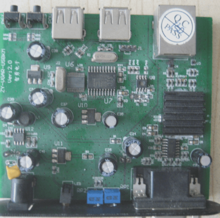
From Schematic to PCB Design Process
- Establish component parameters
- Input principle netlist
- Design parameter settings
- Manual placement
- Manual routing
- Design verification
- Review
- CAM output
Parameter Settings
The spacing between adjacent traces in PCB design is crucial for electrical safety and production efficiency. It is recommended to have wider spacing to ease assembly. The minimum spacing should meet voltage rating requirements. For low trace density, signal line spacing can be increased. In cases of large voltage differences, minimize spacing but increase the gap for critical signals. Typically, trace spacing is set to 8 mils. To prevent pad defects, maintain a distance of at least 1 mm between the inner hole of the PCB pad and the board edge. When connecting thin traces to pads, use a tapered connection to prevent delamination.
PCB Component Layout

Introduction
Proper PCB design is essential for the reliability of electronic equipment. Incorrect PCB design, even with a correct circuit schematic, can lead to signal delays and noise issues. It is crucial to follow best practices in PCB design.
Current Loops in Switching Power Supplies
Switching power supplies consist of four main current loops: power switch AC circuit, output rectifier AC circuit, input signal source current loop, and output load current loop. Correct placement of input and output filter capacitors is vital to prevent AC energy radiation.
Power Switch and Rectifier AC Circuits
The AC circuits of power switches and rectifiers involve high-amplitude trapezoidal currents with significant harmonic components. Proper routing of these AC loops is crucial to minimize electromagnetic interference.
Designing the Switching Power Supply Layout
The layout of a switching power supply should mirror the electrical design. Placing components close together and minimizing trace length and width can reduce impedance and inductance, improving frequency response and reducing interference.
Minimizing Impedance and Inductance
The Importance of PCB Trace Length and Width
The length of a trace impacts its inductance and impedance, while width is inversely related. Longer traces have lower frequencies for sending and receiving electromagnetic waves and are more likely to radiate RF energy. To reduce loop resistance, wider power traces are recommended, with the power trace aligning with the current flow direction alongside the ground trace to enhance noise immunity.
Grounding Strategies for PCB Design
Grounding serves as the common reference point for all current loops in a switching power supply, crucial for interference control. Proper grounding placement is vital to prevent mixing different ground types, which can result in unstable power supply operation.
Design Review Best Practices
After completing PCB routing, a thorough design review is essential to ensure adherence to the designer’s rules and compliance with PCB manufacturing requirements. Key checks include adequate spacing between traces and pads, proper clearance between traces and vias, reasonable distances between component pads and vias, appropriate trace widths for power and ground lines, and the presence of ground planes in sufficient PCB areas.
Exporting PCB Design Files
When exporting Gerber files, ensure output of the routing layer (bottom layer), silk screen layer (top and bottom), bottom solder mask, drilling layer (bottom layer), and NC Drill files. For silk screen layers, avoid selecting “Part Type” and instead choose the top or bottom layer with Outline, Text, and Line. Verify correct configuration of each layer as “Board Outline” in the Layer settings.
If you have any PCB manufacturing requirements, feel free to contact me.


