1. **Design Output**
The PCB design can be exported either to a printer or to a Gerber file. The printer can output the PCB layers, making it easier for both the designer and reviewer to inspect the design. The Gerber file is provided to the board manufacturer for PCB fabrication. The output of the Gerber file is crucial, as it directly affects the success or failure of the design. Below are the key considerations when generating the Gerber file.
a. The layers that need to be output include the signal layers (top, bottom, and internal layers), power layers (VCC and GND), silk screen layers (top and bottom), solder mask layers (top and bottom), and a drilling file (NC Drill).
b. If the power layer is set to Split/Mixed, you must select *Routing* in the Document section of the *Add Document* window. Each time you output the Gerber file, use the *Plane Connect* option in the Pour Manager to pour copper onto the PCB layout. If the power layer is set to *CAM Plane*, select *Plane*. In the *Layer* section, add Layer 25, and choose *Pads* and *Vias* in Layer 25. In the *Device Setup* window, change the aperture value to 199d. When setting up each layer, ensure that the *Board Outline* is selected.
e. For the silk screen layers, do not select *Part Type*. Instead, choose the top or bottom layer and include the outline, text, and lines of the silk screen layer.
f. When configuring the solder mask layers, select vias to indicate that no solder mask should be applied to the vias, or do not select vias to apply a solder mask, depending on the specific requirements of the design.
g. When generating the drilling file, use the default PowerPCB defect save settings and avoid making any changes.
h. Once all Gerber files are output, open and print them using CAM350. Designers and reviewers should check the vias against the *PCB checklist*, as vias are a critical component in multi-layer PCBs. Drilling usually accounts for 30 to 40 percent of the PCB manufacturing cost. Essentially, every hole on the PCB is considered a via. From a functional perspective, vias can be divided into two main categories:
2. **Via Types**
Vias are used for two primary functions:
– Electrical connections between layers
– Fixing or locating components
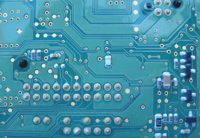
From a process standpoint, vias are typically categorized into three types: blind vias, buried vias, and through vias. Blind vias are located on the top and bottom surfaces of the PCB and have a certain depth. They connect surface traces to underlying inner layers, with hole depths generally limited to a specific ratio relative to the aperture size. Buried vias are connection holes located within the inner layers of the PCB and do not extend to the surface. Both blind and buried vias are created through a special process before lamination, and multiple inner layers may overlap during via formation.
The third type, through vias, pass completely through the PCB and can be used for internal interconnections or for mounting and positioning components. Through vias are generally easier to produce and less expensive than blind or buried vias, making them the most common choice in PCB designs. Unless otherwise specified, vias will be referred to as through vias.
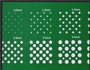
From a design perspective, a via consists of two parts: the drill hole in the center and the pad area surrounding the hole. The size of these two components determines the overall size of the via.
In high-speed, high-density PCB designs, designers generally prefer smaller via holes to maximize available routing space on the board. Additionally, smaller vias help reduce parasitic capacitance, which is beneficial for high-speed circuits. However, reducing via size also increases manufacturing costs and has limitations based on the capabilities of drilling and plating processes. The smaller the hole, the longer it takes to drill, and the more likely it is that the hole will deviate from its center. Furthermore, if the hole depth exceeds six times the drill diameter, it becomes difficult to guarantee uniform copper plating along the hole wall. For example, on a standard 6-layer PCB with a thickness (or hole depth) of around 50 mils, the smallest drill diameter that can typically be achieved by PCB manufacturers is around 8 mils.

**3. Parasitic Capacitance of Vias**
A via inherently has parasitic capacitance with respect to ground. Given that the diameter of the isolation hole on the ground layer of the via is (D_2), the diameter of the via pad is (D_1), the PCB thickness is (T), and the dielectric constant of the substrate is (varepsilon), the parasitic capacitance of the via can be approximately calculated as:
[
C = frac{1.41 varepsilon T D_1}{D_2 – D_1}
]
The parasitic capacitance of the via can increase the rise time of the signal and decrease the overall circuit speed. For example, in a PCB with a thickness of 50 mils, if a via has an inner diameter of 10 mils and a pad diameter of 20 mils, with a distance of 32 mils between the pad and the ground copper area, the parasitic capacitance can be estimated using the formula above:
[
C = frac{1.41 times 4.4 times 0.050 times 0.020}{0.032 – 0.020} = 0.517 text{ pF}
]
The rise time change caused by this capacitance can be approximated as:
[
T_{10-90} = 2.2 C left(frac{Z_0}{2}right) = 2.2 times 0.517 times left(frac{55}{2}right) = 31.28 text{ ps}
]
From these values, it is evident that while the rise-time delay caused by the parasitic capacitance of a single via may not be significant, if multiple vias are used along a trace to switch between layers, the designer should still consider this effect carefully.
**4. Parasitic Inductance of Vias**
Similarly, vias also introduce parasitic inductance. In high-speed digital circuit design, the impact of parasitic inductance often surpasses that of parasitic capacitance. The parasitic series inductance can reduce the effectiveness of bypass capacitors and degrade the filtering performance of the entire power system. The parasitic inductance of a via can be approximated using the following formula:
[
L = 5.08 h left[lnleft(frac{4h}{d}right) – 1right]
]
Where (L) is the inductance of the via, (h) is the via length, and (d) is the diameter of the center drilled hole. From this equation, we can observe that the via diameter has a smaller effect on the inductance, while the via length has the greatest influence. Using the same example as before, the inductance of the via can be calculated as:
[
L = 5.08 times 0.050 left[lnleft(frac{4 times 0.050}{0.010}right) – 1right] = 1
]
If your have any questions about PCB ,please contact me info@wellcircuits.com


