The Importance of Neat and Clear PCB Schematic Diagrams
Creating a PCB schematic diagram that is neat and well-organized is crucial for easy readability and understanding. The design should adhere to national standards to ensure accuracy and clarity.
Key Points for Designing PCB Schematic Diagrams:
- Ensure clear characters, thick lines, and clear subdivisions for easy readability.
- Plan the layout in advance to position graphic symbols uniformly.
- Label each component with a position symbol consisting of text symbols and footnote serial numbers.
- Use position sequence numbers like R1, R2, R3 for resistors and C1, C2, C3 for capacitors.
- Include component details such as number, code, name, model, and quantity in a component list.
- Classify components and follow the sequence numbers for easy assembly.
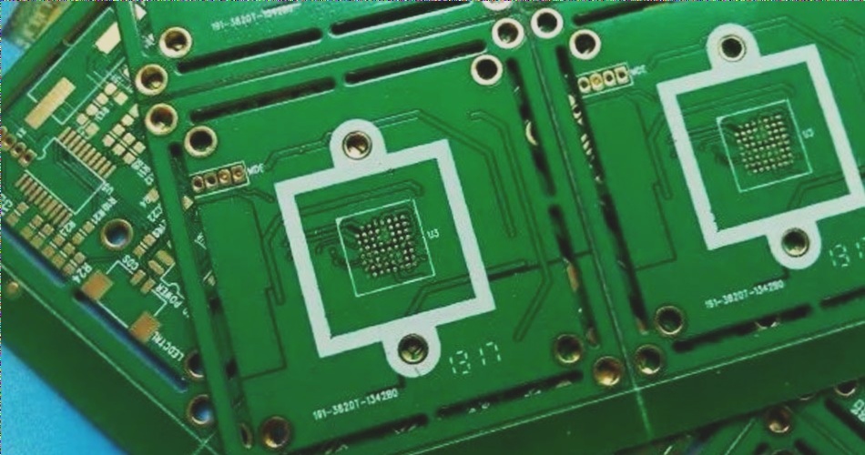
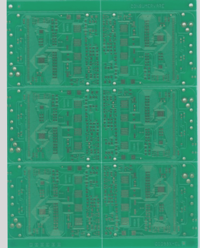
WellCircuits Limited: Your PCB Manufacturing Partner
WellCircuits Limited specializes in manufacturing high-precision PCBs to meet various customer requirements:
- Double-sided and multi-layer PCBs
- Impedance-controlled PCBs
- Blind/buried via PCBs
- Thick copper PCBs
- HDI PCBs
- Backplanes and rigid-flex combinations
- Buried capacitance and resistance PCBs
- Golden Finger PCBs
Trust WellCircuits Limited for all your PCB manufacturing needs.