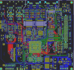
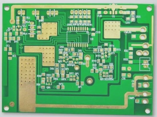
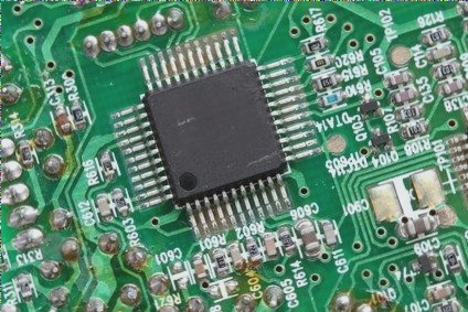
Designing a good PCBA board is crucial for our fundamental operations. Electrical principles and mechanical structure designs are utilized to determine the size and structural shape of the PCBA in accordance with the overall machine structure. The process begins with creating an outline drawing of the SMT printed board, specifying dimensions (length, width, thickness), positions and sizes of structural components, assembly holes, and ensuring adequate edge clearance. This enables circuit designers to conduct wiring within defined parameters.
The choice of assembly method depends on circuit component types, PCB size, and production line equipment capabilities. Principles guiding assembly form selection include process optimization, cost reduction, and product quality enhancement. Initially, establish overall goals for electronic product function, performance metrics, cost considerations, and the machine’s overall dimensions. This positions product performance, quality, and cost effectively.

Under normal circumstances, any product design needs to balance and compromise between performance, manufacturability, and cost. Therefore, when designing, the purpose and grade of the product must be prioritized. PCB board design is intricate, with various unforeseen factors often influencing the overall solution. How can we overcome these challenges? How can we achieve a clean, efficient, and reliable PCBA board design? We are a professional PCB design company, and PCBA board design may seem complex. It involves considering signal direction and energy transmission. However, in essence, the approach can be simplified into two aspects: “how to place” and “how to connect”.
1. Follow the “big and small first, difficult and easy first” layout principle, prioritizing important unit circuits and core components. This is akin to selecting favorite foods at a buffet—limited appetite dictates picking significant items, just as PCB board design space restricts choosing crucial elements.
2. Refer to the schematic diagram when laying out, arranging main components along the primary signal flow direction of the PCB. Layout should meet these criteria: minimize total connection length, ensure key signal lines are the shortest possible, place decoupling capacitors close to IC power supply pins to shorten power-to-ground loops, and prevent accidents.
3. Ensure component arrangement facilitates debugging and repair—avoid crowding small components with larger ones, provide ample space around components for debugging, and evenly distribute heating elements for effective heat dissipation.
4. For structurally similar circuit parts, use symmetrical layout wherever feasible. Optimize layout for uniform distribution, balanced center of gravity, and aesthetic appeal.
5. Orient plug-in components uniformly along the X or Y direction. Ensure consistent orientation for polar discrete components in the X or Y direction to aid production and inspection.
6. Segregate high-voltage, high-current signals from low-current, low-voltage weak signals; separate analog from digital signals, and high-frequency from low-frequency signals. Maintain adequate spacing between high-frequency components to avoid interference.
The “how to place” aspect of layout is primary. “How to connect” is more intricate, prioritizing key signal lines—especially analog signals, small signals, high-speed signals, clock signals, and synchronization signals. Density guides wiring: start from the most complex device area and route from the board’s densest region.
Wiring constitutes a critical phase in PCB product design—rigorous, skill-intensive, and demanding. PCBA layout includes single-sided, double-sided, and multilayer wiring types, achievable via system-provided automatic and manual routing. Despite high routing rates, manual adjustments are often necessary for optimal results. Quality PCBA design significantly impacts interference resistance, necessitating adherence to fundamental design principles and anti-interference requirements for optimal circuit performance.
Printed PCB traces should minimize length; unified component address or data lines should maximize length. High-frequency or dense wiring should employ rounded corners to preserve circuit electrical characteristics. Double-sided wiring mandates perpendicularity to prevent parasitic coupling; use 45° fold lines instead of 90° to reduce signal coupling. Minimize printed wire use for circuit I/O to prevent backflow, and add grounding wires between these to enhance performance.
In dense board wiring, fill mesh copper foil with a grid size of 0.2mm (8mil). Avoid SMD pads through holes to prevent solder joint paste loss; refrain from routing critical signal lines through sockets. Avoid horizontally mounted components under holes to prevent shorts post-soldering. When manually wiring, prioritize ground connections over power lines and avoid signal line loops; if necessary, keep loops minimal. Maintain consistent, maximum spacing between wiring and pads, ensuring smooth transitions to prevent sharp corners.
Adjust wire width based on pad spacing: match pad diameter if centers are closer than pad diameter, decrease width if centers are farther apart. For multiple pads on a wire, spacing should exceed twice the pad diameter. Position common ground near PCB edges to optimize shielding effectiveness; retain copper foil on PCBs to enhance shielding and transmission line characteristics, minimizing distributed capacitance.
For PCBs with multiple ICs, form a common ground ring or net to equalize potential differences and reduce noise tolerance. Align ground and power lines parallel to data flow to suppress noise. Multi-layer PCBA can use internal layers as shielding. PCB power and ground layers effectively function as shielding layers.


