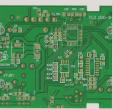
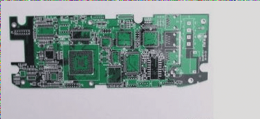
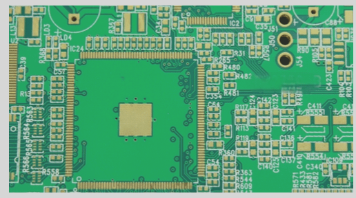
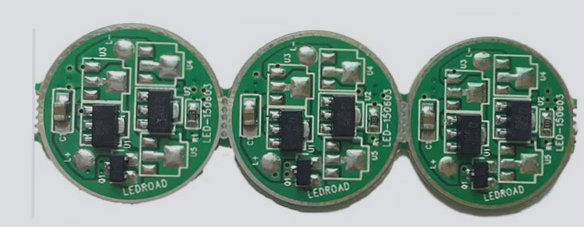
PCB plays a crucial role in enabling the functionality of electronic products, which has made PCB design increasingly important. The performance of PCB design directly impacts the function and cost of electronic products. A well-executed PCB design can help avoid many issues, ensuring smooth product manufacturing and meeting all the requirements of real-world applications.
Among all the factors influencing PCB design, Design for Manufacturing (DFM) is an essential element. It bridges the gap between PCB design and PCB manufacturing, allowing issues to be identified and addressed throughout the entire lifecycle of electronic products. By considering manufacturability during the PCB design phase, the complexity of the design may increase. However, DFM ensures that the product can seamlessly transition into automated production, reducing labor costs and shortening manufacturing time, which ultimately facilitates the timely delivery of the final electronic product.
**PCB Manufacturability**
Given its role in connecting design and manufacturing, manufacturability is a key factor in achieving efficient production, high quality, and cost-effectiveness. The scope of research on PCB manufacturability is broad, and it is generally divided into two main areas: PCB manufacturing and PCB assembly.
**PCB Manufacturing**

1. **PCB Design Considerations**
In PCB manufacturing, several aspects must be carefully considered, including PCB size, shape, process edges, and mark points. If these factors are not fully addressed during the design phase, unless additional measures are implemented, the automated chip placement machine may fail to handle the pre-assembled PCB. Worse, some boards may not even be suitable for manual soldering. This will lead to longer production cycles and increased labor costs.
2. **PCB Size Requirements**
Each chip mounter has specific size requirements for the PCB, which vary according to the machine’s specifications. For instance, the maximum PCB size a chip mounter can accommodate might be 500mm x 450mm, while the minimum size could be 30mm x 30mm. However, this does not mean that smaller components cannot be used. When working with smaller sizes, jigsaw cutting techniques can be employed. When manual installation is required, increased labor costs and an uncontrolled production cycle may result, as chip placement machines will not accept PCBs that are either too large or too small.
Therefore, during the PCB design phase, the size requirements for automated assembly should be carefully considered to ensure the PCB remains within the acceptable size range.
3. **PCB Shape**
Besides size, all chip placement machines have specific requirements regarding the PCB shape. Typically, a rectangular shape is preferred, with the length-to-width ratio ideally being 4:3 or 5:4. Irregularly shaped PCBs require additional measures before SMT assembly, which can increase costs. To avoid this, it’s important to design the PCB with a standard shape that aligns with SMT requirements during the design phase. In cases where an irregular shape is necessary for the final product, a stamp hole can be used to adjust the final PCB shape. After assembly, redundant auxiliary structures can be removed to meet the automatic placement and space requirements.
4. **Process Edges**
To ensure proper handling during automated manufacturing, process edges must be incorporated into the PCB design. A 5mm wide process edge should be reserved around the PCB, free from components and traces. The process edge is typically placed along the short side of the PCB, though it may be positioned on the long side when the aspect ratio exceeds 80%. Once assembly is completed, this craft edge, serving only a production role, can be removed.
5. **Mark Points (Reference Points)**
For PCBs with installed components, mark points must be added to serve as reference points, ensuring precise location identification by assembly equipment. These mark points are essential benchmarks for automated manufacturing.
Typically, two mark points are required for components, and three for the PCB itself. These marks should be positioned along the edge of the PCB, covering all SMT components. The center-to-edge distance of the mark points should be no less than 5mm. For double-sided SMT assemblies, mark points should be placed on both sides of the PCB. If the component density is too high to place the marks on the board itself, they can be positioned along the edge of the process.
6. **PCB Assembly**
PCB assembly, or PCBA, refers to the process of soldering components onto a bare PCB. Automated manufacturing imposes certain requirements on component packaging and layout to ensure smooth assembly.
7. **Component Packaging**
During PCB design, if component packages are not appropriately standardized or if the distance between components is too small, automatic placement machines will struggle to perform the assembly.
To optimize component packaging, it’s important to use professional EDA design software that aligns with international packaging standards. This ensures compatibility, allowing the automated IC placement machine to accurately identify and surface-mount components. The layout should avoid overlapping areas, particularly the bird’s-eye view zone, to facilitate efficient automatic assembly.
8. **Component Layout**
The component layout is a crucial task in PCB design, directly influencing the PCB’s overall appearance and manufacturing complexity.
In the layout process, the assembly surfaces for SMD (Surface Mount Devices) and THD (Through-Hole Devices) components should be determined. The front of the PCB is referred to as the component A side, while the back is the B side. The layout should account for various assembly forms, such as single-layer or double-layer, single- or mixed-package assemblies, and A-side THD and B-side SMD configurations. Each assembly method requires distinct processes and technologies, so selecting the most efficient layout can simplify manufacturing and improve overall production efficiency.
Additionally, the orientation, spacing, heat dissipation, and component height must all be considered during layout.
9. **Component Orientation and Spacing**
Generally, it’s best to maintain consistent component orientation throughout the PCB. The component layout should prioritize minimizing trace lengths. In this context, components with polarity markings should have consistent orientation, while those without polarity markings should be neatly aligned along the X or Y axis. The height of components should generally be limited to 4mm, and the component and PCB alignment should be maintained at a 90° angle.
For efficient soldering and ease of inspection, component spacing should be consistent. Components within the same network should be placed closely, while maintaining a safe distance between different networks based on voltage considerations. Additionally, the silk screen layer must not overlap with pads, as this would hinder component installation.
10. **Heat Dissipation and Component Height**
Given the actual operating temperature of the PCB and the thermal characteristics of the components, thermal management is crucial. The component layout should be optimized for heat dissipation. Fans or heat sinks should be employed where necessary, and appropriate heat sinks should be selected for power components. Heat-sensitive components should be positioned away from heat-generating elements, and taller components should be placed behind shorter ones to prevent thermal interference.
11. **Additional Considerations for PCB DFM (Design for Manufacturing)**
There are many other details that need to be addressed during PCB DFM, and practical experience plays a significant role. For instance, high-speed signal PCB designs often require special attention to impedance, so it’s essential to consult with the PCB manufacturer early in the design phase to determine impedance and layering details. For smaller or densely routed PCBs, it’s advisable to discuss the minimum trace width and through-hole diameter manufacturing capabilities with the PCB manufacturer to ensure successful production.
Among all the factors influencing PCB design, Design for Manufacturing (DFM) is an essential element. It bridges the gap between PCB design and PCB manufacturing, allowing issues to be identified and addressed throughout the entire lifecycle of electronic products. By considering manufacturability during the PCB design phase, the complexity of the design may increase. However, DFM ensures that the product can seamlessly transition into automated production, reducing labor costs and shortening manufacturing time, which ultimately facilitates the timely delivery of the final electronic product.
**PCB Manufacturability**
Given its role in connecting design and manufacturing, manufacturability is a key factor in achieving efficient production, high quality, and cost-effectiveness. The scope of research on PCB manufacturability is broad, and it is generally divided into two main areas: PCB manufacturing and PCB assembly.
**PCB Manufacturing**

1. **PCB Design Considerations**
In PCB manufacturing, several aspects must be carefully considered, including PCB size, shape, process edges, and mark points. If these factors are not fully addressed during the design phase, unless additional measures are implemented, the automated chip placement machine may fail to handle the pre-assembled PCB. Worse, some boards may not even be suitable for manual soldering. This will lead to longer production cycles and increased labor costs.
2. **PCB Size Requirements**
Each chip mounter has specific size requirements for the PCB, which vary according to the machine’s specifications. For instance, the maximum PCB size a chip mounter can accommodate might be 500mm x 450mm, while the minimum size could be 30mm x 30mm. However, this does not mean that smaller components cannot be used. When working with smaller sizes, jigsaw cutting techniques can be employed. When manual installation is required, increased labor costs and an uncontrolled production cycle may result, as chip placement machines will not accept PCBs that are either too large or too small.
Therefore, during the PCB design phase, the size requirements for automated assembly should be carefully considered to ensure the PCB remains within the acceptable size range.
3. **PCB Shape**
Besides size, all chip placement machines have specific requirements regarding the PCB shape. Typically, a rectangular shape is preferred, with the length-to-width ratio ideally being 4:3 or 5:4. Irregularly shaped PCBs require additional measures before SMT assembly, which can increase costs. To avoid this, it’s important to design the PCB with a standard shape that aligns with SMT requirements during the design phase. In cases where an irregular shape is necessary for the final product, a stamp hole can be used to adjust the final PCB shape. After assembly, redundant auxiliary structures can be removed to meet the automatic placement and space requirements.
4. **Process Edges**
To ensure proper handling during automated manufacturing, process edges must be incorporated into the PCB design. A 5mm wide process edge should be reserved around the PCB, free from components and traces. The process edge is typically placed along the short side of the PCB, though it may be positioned on the long side when the aspect ratio exceeds 80%. Once assembly is completed, this craft edge, serving only a production role, can be removed.
5. **Mark Points (Reference Points)**
For PCBs with installed components, mark points must be added to serve as reference points, ensuring precise location identification by assembly equipment. These mark points are essential benchmarks for automated manufacturing.
Typically, two mark points are required for components, and three for the PCB itself. These marks should be positioned along the edge of the PCB, covering all SMT components. The center-to-edge distance of the mark points should be no less than 5mm. For double-sided SMT assemblies, mark points should be placed on both sides of the PCB. If the component density is too high to place the marks on the board itself, they can be positioned along the edge of the process.
6. **PCB Assembly**
PCB assembly, or PCBA, refers to the process of soldering components onto a bare PCB. Automated manufacturing imposes certain requirements on component packaging and layout to ensure smooth assembly.
7. **Component Packaging**
During PCB design, if component packages are not appropriately standardized or if the distance between components is too small, automatic placement machines will struggle to perform the assembly.
To optimize component packaging, it’s important to use professional EDA design software that aligns with international packaging standards. This ensures compatibility, allowing the automated IC placement machine to accurately identify and surface-mount components. The layout should avoid overlapping areas, particularly the bird’s-eye view zone, to facilitate efficient automatic assembly.
8. **Component Layout**
The component layout is a crucial task in PCB design, directly influencing the PCB’s overall appearance and manufacturing complexity.
In the layout process, the assembly surfaces for SMD (Surface Mount Devices) and THD (Through-Hole Devices) components should be determined. The front of the PCB is referred to as the component A side, while the back is the B side. The layout should account for various assembly forms, such as single-layer or double-layer, single- or mixed-package assemblies, and A-side THD and B-side SMD configurations. Each assembly method requires distinct processes and technologies, so selecting the most efficient layout can simplify manufacturing and improve overall production efficiency.
Additionally, the orientation, spacing, heat dissipation, and component height must all be considered during layout.
9. **Component Orientation and Spacing**
Generally, it’s best to maintain consistent component orientation throughout the PCB. The component layout should prioritize minimizing trace lengths. In this context, components with polarity markings should have consistent orientation, while those without polarity markings should be neatly aligned along the X or Y axis. The height of components should generally be limited to 4mm, and the component and PCB alignment should be maintained at a 90° angle.
For efficient soldering and ease of inspection, component spacing should be consistent. Components within the same network should be placed closely, while maintaining a safe distance between different networks based on voltage considerations. Additionally, the silk screen layer must not overlap with pads, as this would hinder component installation.
10. **Heat Dissipation and Component Height**
Given the actual operating temperature of the PCB and the thermal characteristics of the components, thermal management is crucial. The component layout should be optimized for heat dissipation. Fans or heat sinks should be employed where necessary, and appropriate heat sinks should be selected for power components. Heat-sensitive components should be positioned away from heat-generating elements, and taller components should be placed behind shorter ones to prevent thermal interference.
11. **Additional Considerations for PCB DFM (Design for Manufacturing)**
There are many other details that need to be addressed during PCB DFM, and practical experience plays a significant role. For instance, high-speed signal PCB designs often require special attention to impedance, so it’s essential to consult with the PCB manufacturer early in the design phase to determine impedance and layering details. For smaller or densely routed PCBs, it’s advisable to discuss the minimum trace width and through-hole diameter manufacturing capabilities with the PCB manufacturer to ensure successful production.


