Functional Layers of Printed Circuit Boards
-
Signal Layer
The signal layer is crucial for component placement and wiring. Protel DXP typically consists of 30 middle layers, named Mid Layer1 to Mid Layer30, for arranging signal lines. The top and bottom layers are used for component placement and copper deposition.
-
Protective Layer
The protective layer ensures that areas of the circuit board not requiring tinning are not tinned, enhancing operational reliability. The Top Paste and Bottom Paste refer to the top and bottom solder masks, while Top Solder and Bottom Solder act as the solder paste protection layers.
-
Silk Screen Layer
The silk screen layer is utilized for printing component serial numbers, production numbers, and company names on the printed circuit board.
-
Internal Layer
The internal layer functions as a signal wiring layer, with Protel DXP containing 16 internal layers.
-
Other Layers
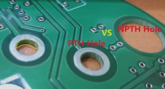
Additional types of layers include the Drill Guide (drilling azimuth layer), which indicates the positions of drilling holes on the printed circuit board.
WellCircuits Limited: Specialized PCB Manufacturer
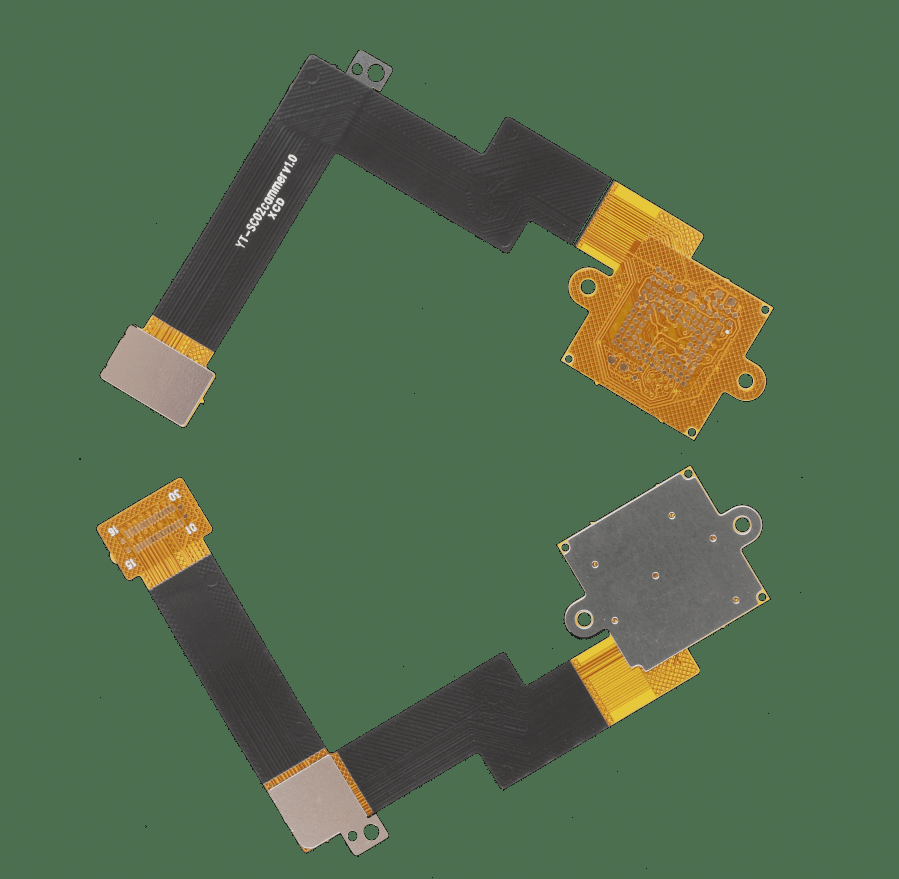
WellCircuits Limited specializes in producing high-precision double-sided, multi-layer, impedance-controlled, blind/buried vias, and thick copper circuit boards. Their product range encompasses HDI, thick copper, backplanes, rigid-flex, buried capacitance, buried resistance, and Golden Finger circuit boards, meeting a wide array of customer needs.


